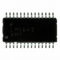
LM5642XMT/NOPB National Semiconductor, LM5642XMT/NOPB Datasheet - Page 16

LM5642XMT/NOPB
Manufacturer Part Number
LM5642XMT/NOPB
Description
IC CONV SYNC DUAL BUCK 28-TSSOP
Manufacturer
National Semiconductor
Series
PowerWise®r
Type
Step-Down (Buck)r
Datasheet
1.LM5642MTCNOPB.pdf
(28 pages)
Specifications of LM5642XMT/NOPB
Internal Switch(s)
No
Synchronous Rectifier
Yes
Number Of Outputs
2
Voltage - Output
1.3 ~ 35 V
Current - Output
20A
Frequency - Switching
375kHz
Voltage - Input
4.5 ~ 36 V
Operating Temperature
-40°C ~ 125°C
Mounting Type
Surface Mount
Package / Case
28-TSSOP
Power - Output
1.1W
For Use With
LM5642EVAL-KIT - BOARD EVALUATION LM5642
Lead Free Status / RoHS Status
Lead free / RoHS Compliant
Other names
*LM5642XMT
*LM5642XMT/NOPB
LM5642XMT
*LM5642XMT/NOPB
LM5642XMT
Available stocks
Company
Part Number
Manufacturer
Quantity
Price
Company:
Part Number:
LM5642XMT/NOPB
Manufacturer:
National Semiconductor
Quantity:
135
www.national.com
tighter control over reverse leakage current across tempera-
ture.
SWITCHING NOISE REDUCTION
Power MOSFETs are very fast switching devices. In syn-
chronous rectifier converters, the rapid increase of drain cur-
rent in the top FET coupled with parasitic inductance will
generate unwanted Ldi/dt noise spikes at the source node of
the FET (SWx node) and also at the VIN node. The magnitude
of this noise will increase as the output current increases. This
parasitic spike noise may produce excessive electromagnetic
interference (EMI), and can also cause problems in device
performance. Therefore, it must be suppressed using one of
the following methods.
When using resistor based current sensing, it is strongly rec-
ommended to add R-C filters to the current sense amplifier
inputs as shown in
to switching noise, especially during heavy load transients
and short on time conditions. The filter components should be
connected as close as possible to the IC.
As shown in
HDRVx pin will slow down the gate drive, thus slowing the rise
and fall time of the top FET, yielding a longer drain current
transition time.
Usually a 3.3Ω to 4.7Ω resistor is sufficient to suppress the
noise. Top FET switching losses will increase with higher re-
sistance values.
Small resistors (1-5 ohms) can also be placed in series with
the CBOOTx pin to effectively reduce switch node ringing. A
CBOOT resistor will slow the rise time of the FET, whereas a
resistor at HDRV will increase both rise and fall times.
CURRENT SENSING AND LIMITING
As shown in
of the current sense amplifier. Current sensing is accom-
plished either by sensing the Vds of the top FET or by sensing
the voltage across a current sense resistor connected from
VIN to the drain of the top FET. The advantages of sensing
current across the top FET are reduced parts count, cost and
power loss.
The R
and voltage as a sense resistor, hence great care must be
used in layout for V
30V, the maximum recommended output current is 5A per
channel.
Keeping the differential current-sense voltage below 200mV
ensures linear operation of the current sense amplifier. There-
fore, the R
must be small enough so that the current sense voltage does
not exceed 200 mV when the top FET is on. There is a leading
edge blanking circuit that forces the top FET on for at least
166ns. Beyond this minimum on time, the output of the PWM
comparator is used to turn off the top FET. Additionally, a
DS-ON
DS-ON
of the top FET is not as stable over temperature
Figure
FIGURE 6. HDRV Series Resistor
Figure
of the top FET or the current sense resistor
DS
Figure
7, the KSx and RSNSx pins are the inputs
sensing circuits. At input voltages above
6, adding a resistor in series with the
7. This will reduce the susceptibility
20060109
16
minimum voltage of at least 50 mV across Rsns is recom-
mended to ensure a high SNR at the current sense amplifier.
Assuming a maximum of 200 mV across Rsns, the current
sense resistor can be calculated as follows:
where Imax is the maximum expected load current, including
overload multiplier (ie:120%), and Irip is the inductor ripple
current (See Equation 17). The above equation gives the
maximum allowable value for Rsns. Conduction losses will
increase with larger Rsns, thus lowering efficiency.
The peak current limit is set by an external resistor connected
between the ILIMx pin and the KSx pin. An internal 10 µA
current sink on the ILIMx pin produces a voltage across the
resistor to set the current limit threshold which is then com-
pared to the current sense voltage. A 10 nF capacitor across
this resistor is required to filter unwanted noise that could im-
properly trip the current limit comparator.
Current limit is activated when the inductor current is high
enough to cause the voltage at the RSNSx pin to be lower
than that of the ILIMx pin. This toggles the Ilim comparator,
thus turning off the top FET immediately. The comparator is
disabled when the top FET is turned off and during the leading
edge blanking time. The equation for current limit resistor,
R
Where Ilim is the load current at which the current limit com-
parator will be tripped.
When sensing current across the top FET, replace Rsns with
the R
that the minimum current limit will not be less than Imax. It is
recommended that a 1% tolerance resistor be used.
When sensing across the top FET (V
show more variation than a current-sense resistor, largely due
to temperature variation. R
temperature according to a specific temperature coefficient.
Refer to the FET manufacturer's datasheet to determine the
range of R
Component Selection section (Equation 27) for a calculation
of maximum R
lim
, is as follows:
DS-ON
FIGURE 7. Current Sense and Current Limit
DS-ON
of the FET. This calculated Rlim value guarantees
DS-ON
values over operating temperature or see the
. This will prevent R
DS-ON
will increase proportional to
DS
DS-ON
sensing), R
20060110
variations from
DS-ON
will
(3)
(4)


