LM5642XMT/NOPB National Semiconductor, LM5642XMT/NOPB Datasheet - Page 4
LM5642XMT/NOPB
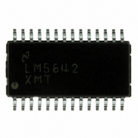
Manufacturer Part Number
LM5642XMT/NOPB
Description
IC CONV SYNC DUAL BUCK 28-TSSOP
Manufacturer
National Semiconductor
Series
PowerWise®r
Type
Step-Down (Buck)r
Datasheet
1.LM5642MTCNOPB.pdf
(28 pages)
Specifications of LM5642XMT/NOPB
Internal Switch(s)
No
Synchronous Rectifier
Yes
Number Of Outputs
2
Voltage - Output
1.3 ~ 35 V
Current - Output
20A
Frequency - Switching
375kHz
Voltage - Input
4.5 ~ 36 V
Operating Temperature
-40°C ~ 125°C
Mounting Type
Surface Mount
Package / Case
28-TSSOP
Power - Output
1.1W
For Use With
LM5642EVAL-KIT - BOARD EVALUATION LM5642
Lead Free Status / RoHS Status
Lead free / RoHS Compliant
Other names
*LM5642XMT
*LM5642XMT/NOPB
LM5642XMT
*LM5642XMT/NOPB
LM5642XMT
Available stocks
Company
Part Number
Manufacturer
Quantity
Price
Company:

Part Number:
LM5642XMT/NOPB
Manufacturer:
National Semiconductor
Quantity:
135


www.national.com
System
ΔV
V
I
VLIN5
V
I
I
I
V
V
V
I
I
V
V
VIN
CL
ss_SC1
ss_SK1
sc_uvdelay
sk_uvdelay
FB1_FB2
CLos
ON_SS1
ON_SS2
SSTO
UVDelay
UVP
Absolute Maximum Ratings
If Military/Aerospace specified devices are required,
please contact the National Semiconductor Sales Office/
Distributors for availability and specifications.
Electrical Characteristics
Unless otherwise specified, V
the specified operating junction temperature range, (-40°C to +125°C, if not otherwise specified). Specifications appearing in plain
type are measured using low duty cycle pulse testing with T
test, or statistical analysis.
Symbol
OUT
Voltages from the indicated pins to SGND/PGND:
VIN, ILIM1, ILIM2, KS1, KS2
SW1, SW2, RSNS1, RSNS2
FB1, FB2, VDD1, VDD2
SYNC, COMP1, COMP2, UV
Delay
ON/SS1, ON/SS2
CBOOT1, CBOOT2
CBOOT1 to SW1, CBOOT2
to SW2
LDRV1, LDRV2
HDRV1 to SW1, HDRV2 to
SW2
HDRV1 to CBOOT1, HDRV2
to CBOOT2
, I
, I
/V
,
ss_SC2
ss_SK2
OUT
Load Regulation
Line Regulation
Feedback Voltage
Input Supply Current
VLIN5 Output Voltage
Current Limit Comparator
Offset (VILIMX −VRSNSX)
Current Limit Sink Current
Soft-Start Source Current
Soft-Start Sink Current
Soft-Start On Threshold
Soft-Start Timeout
Threshold
UV_DELAY Source
Current
UV_DELAY Sink Current
UV_DELAY Threshold
Voltage
FB1, FB2, Under Voltage
Protection Latch Threshold
Hysteresis
(Note
Parameter
2)
IN
= 28V, GND = PGND = 0V, VLIN5 = VDD1 = VDD2. Limits appearing in boldface type apply over
−0.3V to (VLIN5 +0.3)V
−0.3V to (VLIN5 +0.6)V
−0.3V to (VDD+0.3)V
−0.3 to (V
VIN = 28V, V
5.5V
5.5V
-20°C to 85°C
V
5.5V
Shutdown
V
IVLIN5 = 0 to 25mA,
5.5V
V
V
V
(Note
UV-DELAY = 2V
UV-DELAY = 0.4V
As a percentage of nominal output voltage
(falling edge)
ON_SSx
ON_SS1
IN
ON_ss1
ON_ss1
−0.3V to 38V
= 6V
−0.3V to 6V
−0.3V to 7V
≤
≤
≤
≤
9)
(Note
IN
VIN
VIN
VIN
VIN
= V
= V
> 2V
= V
+ 0.3)V
−0.3V
+0.3V
(Note
ON_ss2
ON_ss2
≤
≤
≤
≤
ON_SS2
1)
43V
compx
36V, V
36V
36V
36V
Conditions
8)
A
= 1.5V (on)
= 1.5V
= 0V
= 0.5V to 1.5V
= 25°C
compx
4
=1.25V
Operating Ratings
(Note
VIN (VLIN5 tied to VIN)
VIN (VIN and VLIN5 separate)
Junction Temperature
Power Dissipation (T
C),
(Note
Ambient Storage Temp.
Range
Soldering Dwell Time, Temp.
ESD Rating
TSSOP
eTSSOP
(Note
6),
Wave
Infrared
Vapor Phase
3)
(Note
4)
(Note
7). Min/Max limits are guaranteed by design,
1.2154
1.2179
4.70
Min
8.4
0.5
0.7
0.2
5)
75
2
2
A
= 25°
1.2364
1.2364
(Note
0.04
0.04
1.12
0.48
80.7
Typ
1.1
9.9
2.4
5.5
3.4
2.3
3.7
50
±2
5
5
1)
−65°C to +150°C
1.2574
1.2549
−40°C to +125°C
±7.0
Max
5.30
11.4
110
10sec, 240°C
75sec, 219°C
2.0
5.0
1.4
1.2
10
86
4 sec, 260°C
9
4.5V to 5.5V
5.5V to 36V
1.1W
3.4W
2kV
Units
mA
mV
mA
µA
µA
µA
µA
µA
%
%
%
%
V
V
V
V
V
Related parts for LM5642XMT/NOPB
Image
Part Number
Description
Manufacturer
Datasheet
Request
R

Part Number:
Description:
IC,SMPS CONTROLLER,CURRENT-MODE,TSSOP,28PIN,PLASTIC
Manufacturer:
National Semiconductor
Datasheet:
Part Number:
Description:
National Semiconductor [8-Bit D/A Converter]
Manufacturer:
National Semiconductor
Datasheet:
Part Number:
Description:
National Semiconductor [Media Coprocessor]
Manufacturer:
National Semiconductor
Datasheet:
Part Number:
Description:
Digitally Controlled Tone and Volume Circuit with Stereo Audio Power Amplifier, Microphone Preamp Stage and National 3D Sound
Manufacturer:
National Semiconductor
Datasheet:
Part Number:
Description:
Digitally Controlled Tone and Volume Circuit with Stereo Audio Power Amplifier, Microphone Preamp Stage and National 3D Sound
Manufacturer:
National Semiconductor
Datasheet:
Part Number:
Description:
AC97 Rev 2 Codec with Sample Rate Conversion and National 3D Sound
Manufacturer:
National Semiconductor
Part Number:
Description:
Manufacturer:
National Semiconductor
Datasheet:
Part Number:
Description:
Manufacturer:
National Semiconductor
Datasheet:
Part Number:
Description:
General Purpose, Low Voltage, Low Power, Rail-to-Rail Output Operational Amplifiers
Manufacturer:
National Semiconductor
Datasheet:
Part Number:
Description:
8-bit 20 MSPS flash A/D converter.
Manufacturer:
National Semiconductor
Datasheet:
Part Number:
Description:
Low Noise Quad Operational Amplifier
Manufacturer:
National Semiconductor
Datasheet:
Part Number:
Description:
Quad Differential Line Receivers
Manufacturer:
National Semiconductor
Datasheet:
Part Number:
Description:
Quad High Speed Trapezoidal? Bus Transceiver
Manufacturer:
National Semiconductor
Datasheet:
Part Number:
Description:
Dual Line Receiver
Manufacturer:
National Semiconductor
Datasheet: