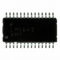
LM5642XMT/NOPB National Semiconductor, LM5642XMT/NOPB Datasheet - Page 19

LM5642XMT/NOPB
Manufacturer Part Number
LM5642XMT/NOPB
Description
IC CONV SYNC DUAL BUCK 28-TSSOP
Manufacturer
National Semiconductor
Series
PowerWise®r
Type
Step-Down (Buck)r
Datasheet
1.LM5642MTCNOPB.pdf
(28 pages)
Specifications of LM5642XMT/NOPB
Internal Switch(s)
No
Synchronous Rectifier
Yes
Number Of Outputs
2
Voltage - Output
1.3 ~ 35 V
Current - Output
20A
Frequency - Switching
375kHz
Voltage - Input
4.5 ~ 36 V
Operating Temperature
-40°C ~ 125°C
Mounting Type
Surface Mount
Package / Case
28-TSSOP
Power - Output
1.1W
For Use With
LM5642EVAL-KIT - BOARD EVALUATION LM5642
Lead Free Status / RoHS Status
Lead free / RoHS Compliant
Other names
*LM5642XMT
*LM5642XMT/NOPB
LM5642XMT
*LM5642XMT/NOPB
LM5642XMT
Available stocks
Company
Part Number
Manufacturer
Quantity
Price
Company:
Part Number:
LM5642XMT/NOPB
Manufacturer:
National Semiconductor
Quantity:
135
Maximum ESR criterion can be used when the associated
capacitance is high enough, otherwise more capacitors than
the number determined by this criterion should be used in
parallel.
MINIMUM CAPACITANCE CALCULATION
In a switch mode power supply, the minimum output capaci-
tance is typically dictated by the load transient requirement.
If there is not enough capacitance, the output voltage excur-
sion will exceed the maximum allowed value even if the
maximum ESR requirement is met. The worst-case load tran-
sient is an unloading transient that happens when the input
voltage is the highest and when the current switching cycle
has just finished. The corresponding minimum capacitance is
calculated as follows:
Notice it is already assumed the total ESR, Re, is no greater
than Re_max, otherwise the term under the square root will
be a negative value. Also, it is assumed that L has already
been selected, therefore the minimum L value should be cal-
culated before C
below). Example: Re = 20 mΩ, Vnom = 5V, ΔVc_s = 160 mV,
ΔIc_s = 3A, L = 8 µH
Generally speaking, C
ΔIc_s, and L, but with increasing Vnom and ΔVc_s.
Inductor Selection
The size of the output inductor can be determined from the
desired output ripple voltage, Vrip, and the impedance of the
output capacitors at the switching frequency. The equation to
determine the minimum inductance value is as follows:
In the above equation, Re is used in place of the impedance
of the output capacitors. This is because in most cases, the
impedance of the output capacitors at the switching frequency
is very close to Re. In the case of ceramic capacitors, replace
Re with the true impedance at the switching frequency.
Example: Vin = 36V, Vo = 3.3V, V
F = 200 kHz.
The actual selection process usually involves several itera-
tions of all of the above steps, from ripple voltage selection,
to capacitor selection, to inductance calculations. Both the
highest and the lowest input and output voltages and load
transient requirements should be considered. If an induc-
tance value larger than Lmin is selected, make sure that the
Cmin requirement is not violated.
Priority should be given to parameters that are not flexible or
more costly. For example, if there are very few types of ca-
pacitors to choose from, it may be a good idea to adjust the
inductance value so that a requirement of 3.2 capacitors can
be reduced to 3 capacitors.
min
and after Re (see Inductor Selection
min
decreases with decreasing Re,
RIP
= 60 mV, Re = 20 mΩ,
(13)
(14)
(15)
(16)
19
Since inductor ripple current is often the criterion for selecting
an output inductor, it is a good idea to double-check this value.
The equation is:
Also important is the ripple content, which is defined by Irip /
Inom. Generally speaking, a ripple content of less than 50%
is ok. Larger ripple content will cause too much power loss in
the inductor.
Example: Vin = 36V, Vo = 3.3V, F = 200 kHz, L = 5 µH, 3A
max I
3A is 100% ripple which is too high.
In this case, the inductor should be reselected on the basis of
ripple current.
Example: 40% ripple, 40% • 3A = 1.2A
When choosing the inductor, the saturation current should be
higher than the maximum peak inductor current and the RMS
current rating should be higher than the maximum load cur-
rent.
Input Capacitor Selection
The fact that the two switching channels of the LM5642 are
180° out of phase will reduce the RMS value of the ripple cur-
rent seen by the input capacitors. This will help extend input
capacitor life span and result in a more efficient system. Input
capacitors must be selected that can handle both the maxi-
mum ripple RMS current at highest ambient temperature as
well as the maximum input voltage. In applications in which
output voltages are less than half of the input voltage, the
corresponding duty cycles will be less than 50%. This means
there will be no overlap between the two channels' input cur-
rent pulses. The equation for calculating the maximum total
input ripple RMS current for duty cycles under 50% is:
where I1 is maximum load current of Channel 1, I2 is the
maximum load current of Channel 2, D1 is the duty cycle of
Channel 1, and D2 is the duty cycle of Channel 2.
Example: Imax_1 = 3.6A, Imax_2 = 3.6A, D1 = 0.42, and D2
= 0.275
Choose input capacitors that can handle 1.66A ripple RMS
current at highest ambient temperature. In applications where
output voltages are greater than half the input voltage, the
corresponding duty cycles will be greater than 50%, and there
will be overlapping input current pulses. Input ripple current
OUT
www.national.com
(17)
(18)
(19)
(20)
(21)
(22)


