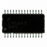
LM5642XMT/NOPB National Semiconductor, LM5642XMT/NOPB Datasheet - Page 22

LM5642XMT/NOPB
Manufacturer Part Number
LM5642XMT/NOPB
Description
IC CONV SYNC DUAL BUCK 28-TSSOP
Manufacturer
National Semiconductor
Series
PowerWise®r
Type
Step-Down (Buck)r
Datasheet
1.LM5642MTCNOPB.pdf
(28 pages)
Specifications of LM5642XMT/NOPB
Internal Switch(s)
No
Synchronous Rectifier
Yes
Number Of Outputs
2
Voltage - Output
1.3 ~ 35 V
Current - Output
20A
Frequency - Switching
375kHz
Voltage - Input
4.5 ~ 36 V
Operating Temperature
-40°C ~ 125°C
Mounting Type
Surface Mount
Package / Case
28-TSSOP
Power - Output
1.1W
For Use With
LM5642EVAL-KIT - BOARD EVALUATION LM5642
Lead Free Status / RoHS Status
Lead free / RoHS Compliant
Other names
*LM5642XMT
*LM5642XMT/NOPB
LM5642XMT
*LM5642XMT/NOPB
LM5642XMT
Available stocks
Company
Part Number
Manufacturer
Quantity
Price
Company:
Part Number:
LM5642XMT/NOPB
Manufacturer:
National Semiconductor
Quantity:
135
www.national.com
A second zero can also be added with a resistor in series with
Cc2. If used, this zero should be placed at fn, where the con-
trol to output gain rolls off at -40dB/dec. Generally, fn will be
well below the 0dB level and thus will have little effect on sta-
bility. Rc2 can be calculated with the following equation:
PCB Layout Considerations
To produce an optimal power solution with the LM5642 series,
good layout and design of the PCB are as important as the
component selection. The following are several guidelines to
aid in creating a good layout.
KELVIN TRACES FOR SENSE LINES
When using the current sense resistor to sense the load cur-
rent connect the KS pin using a separate trace to VIN, as
close as possible to the current-sense resistor. The RSNS pin
should be connected using a separate trace to the low-side
of the current sense resistor. The traces should be run parallel
to each other to give common mode rejection. Although it can
FIGURE 13. Compensation Network
20060174
(38)
(39)
22
be difficult in a compact design, these traces should stay away
from the output inductor and switch node if possible, to avoid
coupling stray flux fields. When a current-sense resistor is not
used the KS pin should be connected as close as possible to
the drain node of the upper MOSFET and the RSNS pin
should be connected as close as possible to the source of the
upper MOSFET using Kelvin traces. To further help minimize
noise pickup on the sense lines is to use RC filtering on the
KS and RSNS pins.
SEPARATE PGND AND SGND
Good layout techniques include a dedicated ground plane,
usually on an internal layer. Signal level components like the
compensation and feedback resistors should be connected to
a section of this internal SGND plane. The SGND section of
the plane should be connected to the power ground at only
one point. The best place to connect the SGND and PGND is
right at the PGND pin..
MINIMIZE THE SWITCH NODE
The plane that connects the power FETs and output inductor
together radiates more EMI as it gets larger. Use just enough
copper to give low impedance to the switching currents,
preferably in the form of a wide, but short, trace run.
LOW IMPEDANCE POWER PATH
The power path includes the input capacitors, power FETs,
output inductor, and output capacitors. Keep these compo-
nents on the same side of the PCB and connect them with
thick traces or copper planes (shapes) on the same layer.
Vias add resistance and inductance to the power path, and
have relatively high impedance connections to the internal
planes. If high switching currents must be routed through vias
and/or internal planes, use multiple vias in parallel to reduce
their resistance and inductance. The power components
should be kept close together. The longer the paths that con-
nect them, the more they act as antennas, radiating unwanted
EMI.
Please see AN-1229 for further PCB layout considerations.


