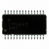
LM5642XMT/NOPB National Semiconductor, LM5642XMT/NOPB Datasheet - Page 21

LM5642XMT/NOPB
Manufacturer Part Number
LM5642XMT/NOPB
Description
IC CONV SYNC DUAL BUCK 28-TSSOP
Manufacturer
National Semiconductor
Series
PowerWise®r
Type
Step-Down (Buck)r
Datasheet
1.LM5642MTCNOPB.pdf
(28 pages)
Specifications of LM5642XMT/NOPB
Internal Switch(s)
No
Synchronous Rectifier
Yes
Number Of Outputs
2
Voltage - Output
1.3 ~ 35 V
Current - Output
20A
Frequency - Switching
375kHz
Voltage - Input
4.5 ~ 36 V
Operating Temperature
-40°C ~ 125°C
Mounting Type
Surface Mount
Package / Case
28-TSSOP
Power - Output
1.1W
For Use With
LM5642EVAL-KIT - BOARD EVALUATION LM5642
Lead Free Status / RoHS Status
Lead free / RoHS Compliant
Other names
*LM5642XMT
*LM5642XMT/NOPB
LM5642XMT
*LM5642XMT/NOPB
LM5642XMT
Available stocks
Company
Part Number
Manufacturer
Quantity
Price
Company:
Part Number:
LM5642XMT/NOPB
Manufacturer:
National Semiconductor
Quantity:
135
Loop Compensation
The general purpose of loop compensation is to meet static
and dynamic performance requirements while maintaining
stability. Loop gain is what is usually checked to determine
small-signal performance. Loop gain is equal to the product
of control-output transfer function and the feedback transfer
function (the compensation network transfer function). Gen-
erally speaking it is desirable to have a loop gain slope that is
roughly -20dB /decade from a very low frequency to well be-
yond the crossover frequency. The crossover frequency
should not exceed one-fifth of the switching frequency. The
higher the bandwidth, the faster the load transient response
speed will be. However, if the duty cycle saturates during a
load transient, further increasing the small signal bandwidth
will not help. Since the control-output transfer function usually
has very limited low frequency gain, it is a good idea to place
a pole in the compensation at zero frequency, so that the low
frequency gain will be relatively large. A large DC gain means
high DC regulation accuracy (i.e. DC voltage changes little
with load or line variations). The rest of the compensation
scheme depends highly on the shape of the control-output
plot.
As shown in
consists of one pole (fp), one zero (fz), and a double pole at
fn (half the switching frequency). The following can be done
to create a -20dB /decade roll-off of the loop gain: Place the
first pole at 0Hz, the first zero at fp, the second pole at fz, and
the second zero at fn. The resulting feedback transfer function
is shown in
FIGURE 11. Control-Output Transfer Function
FIGURE 12. Feedback Transfer Function
Figure
Figure
12.
11, the control-output transfer function
20060114
20060112
21
The control-output corner frequencies, and thus the desired
compensation corner frequencies, can be determined ap-
proximately by the following equations:
Since fp is determined by the output network, it will shift with
loading (Ro). It is best to use a minimum Iout value of ap-
proximately 100mA when determining the maximum Ro val-
ue.
Example: Re = 20 mΩ, Co = 100 uF, Romax = 5V/100 mA =
50Ω:
First determine the minimum frequency (fpmin) of the pole
across the expected load range, then place the first compen-
sation zero at or below that value. Once fpmin is determined,
Rc1 should be calculated using:
Where B is the desired gain in V/V at fp (fz1), gm is the
transconductance of the error amplifier, and R1 and R2 are
the feedback resistors. A gain value around 10dB (3.3v/v) is
generally a good starting point.
Example: B = 3.3v/v, gm = 650m, R1 = 20 kKΩ, R2 = 60.4
kΩ:
Bandwidth will vary proportional to the value of Rc1. Next, Cc1
can be determined with the following equation:
Example: fpmin = 995 Hz, Rc1 = 20 kΩ:
The compensation network
low frequency pole which will be close to 0 Hz.
A second pole should also be placed at fz. This pole can be
created with a single capacitor Cc2 and a shorted Rc2 (see
Figure
culated by:
Cc2 may not be necessary, however it does create a more
stable control loop. This is especially important with high load
currents and in current sharing mode.
Example: fz = 80 kHz, Rc1 = 20 kΩ:
13). The minimum value for this capacitor can be cal-
(Figure
13) will also introduce a
www.national.com
(29)
(30)
(31)
(32)
(33)
(34)
(35)
(36)
(37)


