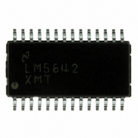
LM5642XMT/NOPB National Semiconductor, LM5642XMT/NOPB Datasheet - Page 17

LM5642XMT/NOPB
Manufacturer Part Number
LM5642XMT/NOPB
Description
IC CONV SYNC DUAL BUCK 28-TSSOP
Manufacturer
National Semiconductor
Series
PowerWise®r
Type
Step-Down (Buck)r
Datasheet
1.LM5642MTCNOPB.pdf
(28 pages)
Specifications of LM5642XMT/NOPB
Internal Switch(s)
No
Synchronous Rectifier
Yes
Number Of Outputs
2
Voltage - Output
1.3 ~ 35 V
Current - Output
20A
Frequency - Switching
375kHz
Voltage - Input
4.5 ~ 36 V
Operating Temperature
-40°C ~ 125°C
Mounting Type
Surface Mount
Package / Case
28-TSSOP
Power - Output
1.1W
For Use With
LM5642EVAL-KIT - BOARD EVALUATION LM5642
Lead Free Status / RoHS Status
Lead free / RoHS Compliant
Other names
*LM5642XMT
*LM5642XMT/NOPB
LM5642XMT
*LM5642XMT/NOPB
LM5642XMT
Available stocks
Company
Part Number
Manufacturer
Quantity
Price
Company:
Part Number:
LM5642XMT/NOPB
Manufacturer:
National Semiconductor
Quantity:
135
prematurely tripping the current limit comparator as the op-
erating temperature increases.
To ensure accurate current sensing using V
cial attention in board layout is required. The KSx and RSNSx
pins require separate traces to form a Kelvin connection at
the corresponding current sense nodes. In addition, the filter
components R14, R16, C14, C15 should be removed.
INPUT UNDER VOLTAGE LOCKOUT (UVLO)
The input under-voltage lock out threshold, which is sensed
via the VLIN5 internal LDO output, is 4.0V (typical). Below this
threshold, both HDRVx and LDRVx will be turned off and the
internal 480Ω MOSFETs will be turned on to discharge the
output capacitors through the SWx pins. When the input volt-
age is below the UVLO threshold, the ON/SS pins will sink
5mA to discharge the soft start capacitors and turn off both
channels. As the input voltage increases again above 4.0V,
UVLO will be de-activated, and the device will restart through
a normal soft start phase. If the voltage at VLIN5 remains be-
low 4.5V, but above the 4.0V UVLO threshold, the device
cannot be guaranteed to operate within specification.
If the input voltage is between 4.0V and 5.2V, the VLIN5 pin
will not regulate, but will follow approximately 200 mV below
the input voltage.
DUAL-PHASE PARALLEL OPERATION
In applications with high output current demand, the two
switching channels can be configured to operate as a two
phase converter to provide a single output voltage with cur-
rent sharing between the two switching channels. This ap-
proach greatly reduces the stress and heat on the output
stage components while lowering input ripple current. The in-
ductor ripple currents also cancel to a varying degree which
results in lowered output ripple voltage.
example of a typical two-phase circuit. Because precision
current sense is the primary design criteria to ensure accurate
current sharing between the two channels, both channels
must use external sense resistors for current sensing. To
minimize the error between the error amplifiers of the two
channels, tie the feedback pins FB1 and FB2 together and
connect to a single voltage divider for output voltage sensing.
Also, tie the COMP1 and COMP2 together and connect to the
compensation network. ON/SS1 and ON/SS2 must be tied
together to enable and disable both channels simultaneously.
EXTERNAL FREQUENCY SYNC
The LM5642 series has the ability to synchronize to external
sources in order to set the switching frequency. This allows
the LM5642 to use frequencies from 150 kHz to 250 kHz and
the LM5642X to use frequencies from 200 kHz to 500 kHz.
Lowering the switching frequency allows a smaller minimum
duty cycle, DMIN, and hence a greater range between input
and output voltage. Increasing switching frequency allows the
use of smaller output inductors and output capacitors (See
Component Selection). In general, synchronizing all the
switching frequencies in multi-converter systems makes fil-
tering of the switching noise easier.
The sync input can be from a system clock, from another
switching converter in the system, or from any other periodic
signal with a logic low-level less than 1.4V and a logic high
level greater than 2V. Both CMOS and TTL level inputs are
acceptable.
The LM5642 series uses a fixed delay between Channel 1
and Channel 2. The nominal switching frequency of 200kHz
for the LM5642 corresponds to a switching period of 5µs.
Channel 2 always turns its high-side switch on 2.5µs after
Figure 2
DS
sensing, spe-
shows an
17
Channel 1
to a frequency other than 200kHz, the switching period is re-
duced or increased, while the fixed delay between Channel 1
and Channel 2 remains constant. The phase difference be-
tween channels is therefore no longer 180°. At the extremes
of the sync range, the phase difference drops to 135°
8
is a reduction in the maximum duty cycle of one channel that
will not overlap the duty cycle of the other. As shown in Input
Capacitor Selection section, when the duty cycle D1 for Chan-
nel 1 overlaps the duty cycle D2 for Channel 2, the input rms
current increases, requiring more input capacitors or input
capacitors with higher ripple current ratings. The new, re-
duced maximum duty cycle can be calculated by multiplying
the sync frequency (in Hz) by 2.5x10
onds). The same logic applies to the LM5642X. However the
LM5642X has a nominal switching frequency of 375kHz
which corresponds to a period of 2.67µs. Therefore channel
2 of the LM5642X always begins it's period after 1.33µs.
At a sync frequency of 150 kHz, for example, the maximum
duty cycle for Channel 1 that will not overlap Channel 2 would
be 37.5%. At 250 kHz, it is the duty cycle for Channel 2 that
is reduced to a D
Component Selection
OUTPUT VOLTAGE SETTING
The output voltage for each channel is set by the ratio of a
voltage divider as shown in
be determined by the following equation:
(b) and
Figure 8
FIGURE 8. Period Fixed Delay Example
Figure 8
D
MAX
MAX
(c). The result of this lower phase difference
(a). When the converter is synchronized
= FSYNC
of 37.5%.
Figure
*
2.5x10
9. The resistor values can
-6
-6
(the fixed delay in sec-
20060195
www.national.com
Figure
(5)


