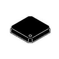
ADP3290JCPZ-RL ON Semiconductor, ADP3290JCPZ-RL Datasheet - Page 14

ADP3290JCPZ-RL
Manufacturer Part Number
ADP3290JCPZ-RL
Description
IC CTLR BUCK SW REG 40-LFCSP
Manufacturer
ON Semiconductor
Type
Step-Down (Buck)r
Datasheet
1.ADP3290JCPZ-RL.pdf
(30 pages)
Specifications of ADP3290JCPZ-RL
Internal Switch(s)
No
Synchronous Rectifier
Yes
Number Of Outputs
4
Voltage - Output
0.5 ~ 1.6 V
Frequency - Switching
250kHz ~ 4MHz
Voltage - Input
12V
Operating Temperature
0°C ~ 85°C
Mounting Type
Surface Mount
Package / Case
40-LFCSP
Output Voltage
0.5 V to 1.6 V
Output Current
500 uA
Input Voltage
- 0.3 V to + 6.3 V
Supply Current
25 mA
Switching Frequency
450 kHz
Mounting Style
SMD/SMT
Maximum Operating Temperature
+ 85 C
Minimum Operating Temperature
0 C
Lead Free Status / RoHS Status
Lead free / RoHS Compliant
Current - Output
-
Power - Output
-
Lead Free Status / Rohs Status
Lead free / RoHS Compliant
Available stocks
Company
Part Number
Manufacturer
Quantity
Price
UVLO or EN is less than their respective thresholds, the
ADP3290 is disabled. This holds the PWM outputs at
ground, shorts the DELAY capacitor to ground, and the
forces PWRGD and OD signals low.
to the OD input of the external driver for the phase that is
always on while the ODN pin should be connected to the OD
input on the external drivers of the phases that are shut off
during low−power operation. Grounding OD and ODN
disable the drivers such that both DRVH and DRVL are
grounded. This feature is important in preventing the
discharge of the output capacitors when the controller is shut
off. If the driver outputs are not disabled, a negative voltage
can be generated during output due to the high current
discharge of the output capacitors through the inductors.
VR11.1 VID Codes
In the application circuit, the OD pin should be connected
OUTPUT(V)
1.60000
1.59375
1.58750
1.58125
1.57500
1.56875
1.56250
1.55625
1.55000
1.54375
1.53750
1.53125
1.52500
1.51875
1.51250
1.50625
1.50000
1.49375
1.48750
1.48125
1.47500
1.46875
1.46250
1.45625
1.45000
1.44375
1.43750
1.43125
1.42500
1.41875
1.41250
OFF
OFF
VID7
0
0
0
0
0
0
0
0
0
0
0
0
0
0
0
0
0
0
0
0
0
0
0
0
0
0
0
0
0
0
0
0
0
VID6
0
0
0
0
0
0
0
0
0
0
0
0
0
0
0
0
0
0
0
0
0
0
0
0
0
0
0
0
0
0
0
0
0
http://onsemi.com
VID5
0
0
0
0
0
0
0
0
0
0
0
0
0
0
0
0
0
0
0
0
0
0
0
0
0
0
0
0
0
0
0
0
1
14
Thermal Monitoring
detect when a point on the VR has exceeded a user−defined
temperature. The thermal monitoring circuit requires an
NTC thermistor to be placed between TTSNS and GND.
and into the thermistor. The current source is internally
limited to 5.0 V. An internal circuit compares the TTSNS
voltage to a 0.81 V threshold, and outputs an open−drain
signal at the VRHOT output. Once the voltage on the
TTSNS pin drops below its threshold, the open−drain output
asserts high to signal the system that an overtemperature
event has occurred. Because the TTSNS voltage changes
slowly with respect to time, 55 mV of hysteresis is built into
this comparator. The thermal monitoring circuitry does not
depend on EN and is active when UVLO is above its
threshold. When UVLO is below its threshold, VRHOT is
forced low.
The ADP3290 includes a thermal monitoring circuit to
A fixed current of 120 mA is sourced out of the TTSNS pin
VID4
0
0
0
0
0
0
0
0
0
0
0
0
0
0
0
0
1
1
1
1
1
1
1
1
1
1
1
1
1
1
1
1
0
VID3
0
0
0
0
0
0
0
0
1
1
1
1
1
1
1
1
0
0
0
0
0
0
0
0
1
1
1
1
1
1
1
1
0
VID2
0
0
0
0
1
1
1
1
0
0
0
0
1
1
1
1
0
0
0
0
1
1
1
1
0
0
0
0
1
1
1
1
0
VID1
0
0
1
1
0
0
1
1
0
0
1
1
0
0
1
1
0
0
1
1
0
0
1
1
0
0
1
1
0
0
1
1
0
VID0
0
1
0
1
0
1
0
1
0
1
0
1
0
1
0
1
0
1
0
1
0
1
0
1
0
1
0
1
0
1
0
1
0


