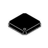
ADP3290JCPZ-RL ON Semiconductor, ADP3290JCPZ-RL Datasheet - Page 8

ADP3290JCPZ-RL
Manufacturer Part Number
ADP3290JCPZ-RL
Description
IC CTLR BUCK SW REG 40-LFCSP
Manufacturer
ON Semiconductor
Type
Step-Down (Buck)r
Datasheet
1.ADP3290JCPZ-RL.pdf
(30 pages)
Specifications of ADP3290JCPZ-RL
Internal Switch(s)
No
Synchronous Rectifier
Yes
Number Of Outputs
4
Voltage - Output
0.5 ~ 1.6 V
Frequency - Switching
250kHz ~ 4MHz
Voltage - Input
12V
Operating Temperature
0°C ~ 85°C
Mounting Type
Surface Mount
Package / Case
40-LFCSP
Output Voltage
0.5 V to 1.6 V
Output Current
500 uA
Input Voltage
- 0.3 V to + 6.3 V
Supply Current
25 mA
Switching Frequency
450 kHz
Mounting Style
SMD/SMT
Maximum Operating Temperature
+ 85 C
Minimum Operating Temperature
0 C
Lead Free Status / RoHS Status
Lead free / RoHS Compliant
Current - Output
-
Power - Output
-
Lead Free Status / Rohs Status
Lead free / RoHS Compliant
Available stocks
Company
Part Number
Manufacturer
Quantity
Price
5000
4500
4000
3500
3000
2500
2000
1500
1000
ELECTRICAL CHARACTERISTICS
Thermal Throttling Control cont.
Power−Good Comparator
Supply
1. All limits at temperature extremes are guaranteed via correction using standard quality control (SQC).
2. Guaranteed by characterization, not tested in production.
3. Guaranteed by design, not tested in production.
TTSNS VRHOT Threshold Voltage
TTSNS Hysteresis
VRHOT Output Low Voltage
Undervoltage Threshold
Overvoltage Threshold
Output Low Voltage
Power−Good Delay Time During
Soft−Start
VID Code Changing
VID Code Static
Crowbar Trip Point
Crowbar Reset Threshold
Crowbar Delay Time VID Code
Changing
VID Code Static
PWM OUTPUTS Output Low Voltage
Output High Voltage
VCC
DC Supply Current
Shunt Turn−On Current
Shunt Turn−On Threshold Voltage
Shunt Turn−Off Voltage
500
0
0
100 200 300
Figure 3. Oscillator Frequency vs. RT
Parameter
400 500 600 700 800 900
RT (kW)
V
V
V
V
V
t
V
V
(V
CROWBAR
V
PWRGD(UV)
PWRGD(OV)
OL(PWRGD)
Symbol
CB(CSREF)
OL(VRHOT)
OL(PWM)
OH(PWM)
SYSTEM
CC
I
V
VCC
CC
= 12 V, FBRTN = GND, T
TYPICAL CHARACTERISTICS
I
Relative to nominal DAC output
Relative to nominal DAC output
I
C
Relative to nominal DAC output
Relative to FBRTN
Overvoltage to PWM going low
I
I
V
V
V
V
VRHOT(SINK)
PWRGD(SINK)
PWM(SINK)
PWM(SOURCE)
SYSTEM
SYSTEM
SYSTEM
SYSTEM
DELAY
http://onsemi.com
1000
= 10 nF
= 12 V, R
= 13.2 V, R
rising
falling
= −400 mA
8
= −4 mA, TTSNS = 5.0 V
= −4 mA
Conditions
= 400 mA
Figure 4. Oscillator Frequency vs. Supply Current
A
5.8
SHUNT
= 0°C to 85°C unless otherwise noted) (Note 1)
SHUNT
= 340 W
= 340 W
6.0
SUPPLY CURRENT (mA)
−400
4.65
6.2
Min
715
100
100
100
305
100
4.0
−350
Typ
760
150
150
150
250
200
150
360
250
400
160
2.0
5.0
5.0
6.5
4.1
50
6
6.4
−300
Max
5.55
805
300
200
300
200
415
500
25
6.6
Unit
mV
mV
mV
mV
mV
mV
mV
mV
mV
mA
mA
ms
ms
ns
ms
ns
V
V
V
V
5000
4500
4000
3500
3000
2500
2000
1500
1000
500
0


