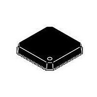
ADP3290JCPZ-RL ON Semiconductor, ADP3290JCPZ-RL Datasheet - Page 5

ADP3290JCPZ-RL
Manufacturer Part Number
ADP3290JCPZ-RL
Description
IC CTLR BUCK SW REG 40-LFCSP
Manufacturer
ON Semiconductor
Type
Step-Down (Buck)r
Datasheet
1.ADP3290JCPZ-RL.pdf
(30 pages)
Specifications of ADP3290JCPZ-RL
Internal Switch(s)
No
Synchronous Rectifier
Yes
Number Of Outputs
4
Voltage - Output
0.5 ~ 1.6 V
Frequency - Switching
250kHz ~ 4MHz
Voltage - Input
12V
Operating Temperature
0°C ~ 85°C
Mounting Type
Surface Mount
Package / Case
40-LFCSP
Output Voltage
0.5 V to 1.6 V
Output Current
500 uA
Input Voltage
- 0.3 V to + 6.3 V
Supply Current
25 mA
Switching Frequency
450 kHz
Mounting Style
SMD/SMT
Maximum Operating Temperature
+ 85 C
Minimum Operating Temperature
0 C
Lead Free Status / RoHS Status
Lead free / RoHS Compliant
Current - Output
-
Power - Output
-
Lead Free Status / Rohs Status
Lead free / RoHS Compliant
Available stocks
Company
Part Number
Manufacturer
Quantity
Price
NOTE:
PIN ASSIGNMENT
32 to 39
22 to 25
27 to 30
Pin No.
10
12
13
14
15
16
17
18
19
20
21
26
31
40
11
1
2
3
4
5
6
7
8
9
True no connect. Printed circuit board traces are allowable.
Mnemonic
CSCOMP
PWM4 to
PWRGD
CSSUM
VRHOT
FBRTN
TRDET
TTSNS
CSREF
SW4 to
VID7 to
DELAY
COMP
PMW1
RAMP
LLINE
IMON
GND
IREF
ODN
VID0
SW1
VCC
ILIM
OD
PSI
EN
SS
FB
RT
Power Supply Enable Input. Pulling this pin to GND disables the PWM outputs and pulls the PWRGD output low.
Power−Good Output. Open−drain output that signals when the output voltage is outside of the proper operating range.
Feedback Return. VID DAC and error amplifier input for remote sensing of the output voltage.
Feedback Input. Error amplifier reference for remote sensing of the output voltage. An external resistor between
this pin and the output voltage sets the no−load offset point.
Error Amplifier Output and Compensation Point.
Soft−Start Delay Setting Input. An external capacitor connected between this pin and GND sets the soft−start
ramp−up time. After startup, pin used to control DVID slew−rate.
Delay Timer Setting Input. An external capacitor connected between this pin and GND sets the overcurrent
latchoff delay time, boot voltage hold time, EN delay time, and PWRGD delay time.
Transient detection output. This pin is pulled low when a load release transient is detected.
VR Hot Output. Active high open−drain output that signals when the temperature of the temperature sensor
connected to TTSNS exceeds the programmed VRHOT temperature threshold.
VR Hot Thermal Throttling Sense Input. An NTC thermistor between this pin and GND is used to remotely sense
the temperature at the desired thermal monitoring point.
Current Sense and Limit Pin. Connecting a resistor from this pin to CSCOMP sets the internal current sensing
signal for current limit and IMON.
Frequency Setting Resistor Input. An external resistor connected between this pin and GND sets the PWM
oscillator frequency.
PWM Ramp Slope Setting Input. An external resistor from the converter input voltage to this pin sets the slope
of the internal PWM ramp.
Output Load Line Programming Input. This pin can be directly connected to CSCOMP, or it can be connected to
the center point of a resistor divider between CSCOMP and CSREF. Connecting LLINE to CSREF disables
positioning.
Current Sense Reference Voltage Input. The voltage on this pin is used as the reference for the current sense
amplifier and the power−good and crowbar functions. This pin should be connected to the common point of the
output inductors.
Current Sense Summing Node. External resistors from each switch node to this pin sum the inductor currents
together to measure the total output current.
Current Sense Compensation Point. A resistor and capacitor from this pin to CSSUM determines the gain of the
current sense amplifier and the positioning loop response time.
Ground. All internal biasing and the logic output signals of the device are referenced to this ground.
Output Disable Logic Output for phase 1. This pin is actively pulled low when the EN input is low or when VCC is
below its UVLO threshold to signal to the Driver IC that the driver high−side and low−side outputs should go low.
Current Reference Input. An external resistor from this pin to ground sets the internal reference current used to
generate I
IMON Total Current Output Pin. A resistor/capacitor from this pin to FBRTN/VSS Sense sets the IMON signal.
Current Balance Inputs. Inputs for measuring the current level in each phase. The SW pins of unused phases
should be left open.
Output Disable Logic output for PSI Operation. This pin is pulled low when PSI is low, otherwise it functions the
same as OD.
Logic−Level PWM Outputs. Each output is connected to the input of an external MOSFET driver such as the
ADP3121. Connecting the PWM4, and/or PWM3 output to VCC causes that phase to turn off, allowing the
ADP3290 to operate as a 2−, 3−, or 4−phase controller.
Supply Voltage for the Device. A 340W resistor should be placed between the 12 V system supply and the VCC
pin. The internal shunt regulator maintains VCC = 5.0 V.
Voltage Identification DAC Inputs. These eight pins are pulled down to GND, providing a Logic 0 if left open.
When in normal operation mode, the DAC output programs the FB regulation voltage from 0.5 V to 1.6 V.
Power State Indicator Input. Pulling this pin low places controller in lower power state operation.
FB
, I
DELAY
, I
SS
, I
CL
, and I
http://onsemi.com
TTSNS
.
5
Description


