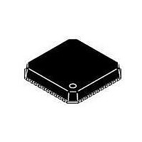
ADP3290JCPZ-RL ON Semiconductor, ADP3290JCPZ-RL Datasheet - Page 29

ADP3290JCPZ-RL
Manufacturer Part Number
ADP3290JCPZ-RL
Description
IC CTLR BUCK SW REG 40-LFCSP
Manufacturer
ON Semiconductor
Type
Step-Down (Buck)r
Datasheet
1.ADP3290JCPZ-RL.pdf
(30 pages)
Specifications of ADP3290JCPZ-RL
Internal Switch(s)
No
Synchronous Rectifier
Yes
Number Of Outputs
4
Voltage - Output
0.5 ~ 1.6 V
Frequency - Switching
250kHz ~ 4MHz
Voltage - Input
12V
Operating Temperature
0°C ~ 85°C
Mounting Type
Surface Mount
Package / Case
40-LFCSP
Output Voltage
0.5 V to 1.6 V
Output Current
500 uA
Input Voltage
- 0.3 V to + 6.3 V
Supply Current
25 mA
Switching Frequency
450 kHz
Mounting Style
SMD/SMT
Maximum Operating Temperature
+ 85 C
Minimum Operating Temperature
0 C
Lead Free Status / RoHS Status
Lead free / RoHS Compliant
Current - Output
-
Power - Output
-
Lead Free Status / Rohs Status
Lead free / RoHS Compliant
Available stocks
Company
Part Number
Manufacturer
Quantity
Price
to the air. Make a mirror image of any pad being used to
heatsink the MOSFETs on the opposite side of the PCB to
achieve the best thermal dissipation in the air around the
board. To further improve thermal performance, use the
largest possible pad area.
a short distance. The output power path is formed by the
current path through the inductor, the output capacitors, and
the load.
should be used as one of the inner layers extending fully
under all the power components.
The output power path should also be routed to encompass
For best EMI containment, a solid power ground plane
http://onsemi.com
29
Signal Circuitry Recommendations
FB pin and the FBRTN pin, which connect to the signal
ground at the load. To avoid differential mode noise pickup
in the sensed signal, the loop area should be small. Thus, the
FB trace and FBRTN trace should be routed adjacent to each
other on top of the power ground plane back to the
controller.
connected as close as possible to the inductor. The CSREF
signal should be connected to the output voltage at the
nearest inductor to the controller.
The output voltage is sensed and regulated between the
The feedback traces from the switch nodes should be


