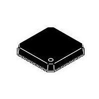
ADP3290JCPZ-RL ON Semiconductor, ADP3290JCPZ-RL Datasheet - Page 20

ADP3290JCPZ-RL
Manufacturer Part Number
ADP3290JCPZ-RL
Description
IC CTLR BUCK SW REG 40-LFCSP
Manufacturer
ON Semiconductor
Type
Step-Down (Buck)r
Datasheet
1.ADP3290JCPZ-RL.pdf
(30 pages)
Specifications of ADP3290JCPZ-RL
Internal Switch(s)
No
Synchronous Rectifier
Yes
Number Of Outputs
4
Voltage - Output
0.5 ~ 1.6 V
Frequency - Switching
250kHz ~ 4MHz
Voltage - Input
12V
Operating Temperature
0°C ~ 85°C
Mounting Type
Surface Mount
Package / Case
40-LFCSP
Output Voltage
0.5 V to 1.6 V
Output Current
500 uA
Input Voltage
- 0.3 V to + 6.3 V
Supply Current
25 mA
Switching Frequency
450 kHz
Mounting Style
SMD/SMT
Maximum Operating Temperature
+ 85 C
Minimum Operating Temperature
0 C
Lead Free Status / RoHS Status
Lead free / RoHS Compliant
Current - Output
-
Power - Output
-
Lead Free Status / Rohs Status
Lead free / RoHS Compliant
Available stocks
Company
Part Number
Manufacturer
Quantity
Price
for R
a given R
of thermistor available. Also, compute a scaling factor (k)
based on the ratio of the actual thermistor value used relative
to the computed one.
Figure 10. Temperature Compensation Circuit Values
r
(A * B)xr
The following procedure and equations yield values to use
Calculate R
CS2
ADP3290
1. Select an NTC based on type and value. Because
2. Based on the type of NTC, find its relative
3. Find the relative value of R
4. Compute the relative values for R
CS1
PLACE AS CLOSE AS POSSIBLE
A
+
the value is unknown, use a thermistor with a
value close to R
initial tolerance of better than 5%.
resistance value at two temperatures. The
temperatures that work well are 50°C and 90°C.
These resistance values are called
A (R
(R
NTC is always 1 at 25°C.
these temperatures. This is based on the percentage
change needed, which in this example is initially
0.39%/°C. These temperatures are called
r
and
r
for copper, T
r
R
TO NEAREST INDUCTOR
CSCOMP
1
2
1
OR LOW−SIDE MOSFET
, R
TH
CSSUM
CSREF
CS
TH(90°C)
(1/(1 + TC × (T
(1/(1 + TC × (T
= 0.9112 and r
(1 * B)xr
1
CS2
TH(50°C)
using:
xr
value.
TH
2
17
16
15
, and R
* A
C
r
r
= r
CS1
TH
CS1
)/R
k +
TH
)/R
1
1
+
TH(25°C)
* B
+
TH
= 50°C, and T
R
(1 * B)xr
TH(25°C)
× R
CS
1*r
2
1*r
TH(CALCULATED)
(the thermistor value at 25°C) for
R
1
2
C
. The NTC should also have an
= 0.7978.
CS2
1
CS
− 25°C)))
− 25°C))), where TC = 0.0039
TH(ACTUAL)
CS2
1
R
R
). The relative value of the
(1 * A)xr
CS2
CS1
, then select the closest value
TH
1
(1 * A)
) and B
* 1
2
*
R
R
) B
r
CS2
CS
PH1
CS1
r
2
1
*r
required for each of
= 90°C. From this,
SWITCH NODE LINES
2
R
WELL AWAY FROM
A
KEEP THIS PATH
PH2
* (A * B)
POSSIBLE AND
AS SHORT AS
CS2
CS1
(1 * A)
R
, R
PH3
CS2
R
PH4
(eq. 10)
, and
(eq. 11)
(eq. 8)
(eq. 9)
http://onsemi.com
xr
1
20
an available 100 kW thermistor, 0603 size. One such
thermistor is the Vishay NTHS0603N01N1003JR NTC
thermistor with A = 0.3602 and B = 0.09174. From these
values, r
making k = 0.816. Next, find R
and 87.9 kW. Finally, choose the closest 1% resistor values,
which yield a choice of 35.7 kW and 88.7 kW.
Load Line Setting
equal to R
to the CSCOMP pin. When the load line value needs to be
less than 1 mW, two additional resistors are required.
Figure 11 shows the placement of these resistors.
the CSCOMP pin and CSREF pin. This resistor divider is
input into the LLSET pin to set the load line slope R
VR according to the following equation:
factors.
•
In this example, R
Solving for R
For load line values greater than 1 mW, R
The two resistors R
The resistor values for R
The minimum value is based upon the loading of the
CSCOMP pin. This pin’s drive capability is 500 mA and
the majority of this should be allocated to the CSA
feedback. If the current through R
limited to 10% of this (50 mA), the following limit can
be placed for the minimum value for R
ADP3290
5. Calculate values for R
Equation 12 and 13.
CSCOMP
CS1
CSSUM
CSREF
Figure 11. Load Line Setting Resistors
LLINE
O
R
R
, and the LLSET pin can be directly connected
CS1
CS2
= 0.3795, r
17
16
15
14
R
R
TH
+ R
+ R
LL1
O
yields 122.55 kW, so 100 kW is chosen,
+
R
) R
CS
LL1
CS
CS
LL1
R
is calculated to be 114 kW. Look for
CS2
LL1
LL2
and R
R
R
k
LL2
LL1
) R
= 0.7195, and r
(1 * k) ) k
LL2
w
CS1
and R
CS1
LL2
r
I
LL2
50
LIM
CS1
and R
OPTIONAL LOAD LINE
and R
set up a divider between
LL2
LL1
SELECT SWITCH
10
R
R
Q
CSA
CS2
LL
CSA
*6
are limited by two
and R
CS2
LL1
TH
r
using
CS2
CSA
to be 35.3 kW
and R
= 1.075.
LL2
can be set
is
(eq. 14)
(eq. 15)
O
LL2
(eq. 12)
(eq. 13)
of the
:


