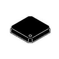
ADP3290JCPZ-RL ON Semiconductor, ADP3290JCPZ-RL Datasheet - Page 26

ADP3290JCPZ-RL
Manufacturer Part Number
ADP3290JCPZ-RL
Description
IC CTLR BUCK SW REG 40-LFCSP
Manufacturer
ON Semiconductor
Type
Step-Down (Buck)r
Datasheet
1.ADP3290JCPZ-RL.pdf
(30 pages)
Specifications of ADP3290JCPZ-RL
Internal Switch(s)
No
Synchronous Rectifier
Yes
Number Of Outputs
4
Voltage - Output
0.5 ~ 1.6 V
Frequency - Switching
250kHz ~ 4MHz
Voltage - Input
12V
Operating Temperature
0°C ~ 85°C
Mounting Type
Surface Mount
Package / Case
40-LFCSP
Output Voltage
0.5 V to 1.6 V
Output Current
500 uA
Input Voltage
- 0.3 V to + 6.3 V
Supply Current
25 mA
Switching Frequency
450 kHz
Mounting Style
SMD/SMT
Maximum Operating Temperature
+ 85 C
Minimum Operating Temperature
0 C
Lead Free Status / RoHS Status
Lead free / RoHS Compliant
Current - Output
-
Power - Output
-
Lead Free Status / Rohs Status
Lead free / RoHS Compliant
Available stocks
Company
Part Number
Manufacturer
Quantity
Price
Thermal Monitor Design
ADP3290 for monitoring the temperature of the VR. A
constant current of 123 mA is sourced out of this pin and runs
through a thermistor network such as the one shown in
Figure 14.
thermistor and sensed inside the IC. When the voltage reaches
1.105V, the VRFAN output gets set. When the voltage
reaches 0.81 V, the VRHOT gets set. This corresponds to
Equation 48.
where:
V
supply (if the 12 V input supply is 12 V ± 5%,
V
V
of the ADP3290. This is specified as 4.75 V. R
shunt resistor value.
NEAR CLOSEST PHASE
IN(MAX)
IN(MAX)
IN(MAX)
The thermistor is used on the TTSENSE input of the
A voltage is generated from this current through the
The maximum power dissipated is calculated using
PLACE THERMISTOR
Figure 14. VR Thermal Monitor Circuit
= 12.6 V; if the 12 V input supply is 12 V ± 10%,
= 13.2 V). V
is the maximum voltage from the 12 V input
P
Figure 15. Typical Shunt Resistor Value and Power Dissipation for Different UVLO Voltage
MAX
+
CC(MIN)
TEMPERATURE
R
V
TTSENSE
IN(MAX)
OPTIONAL
RESISTOR
ADJUST
R
is the minimum V
550
500
450
400
350
300
250
200
150
SHUNT
* V
7.0
CC(MIN)
7.5
P
SHUNT
0.1mF
2
SHUNT
8.0
10
9
CC
VRHOT
TTSNS
ADP3290
(eq. 48)
voltage
http://onsemi.com
8.5
is the
V
IN
9.0
(UVLO)
26
R
SHUNT
R
VRHOT.
~100°C and ~110°C when using the same type of 100 kW
NTC thermistor used in the current sense amplifier.
allows tuning of the trip point temperatures to match the
hottest temperature in the VR, when the thermistor itself is
directly sensing a proportionately lower temperature.
Setting this resistor value is best accomplished with a
variable resistor during thermal validation and then fixing
this value for the final design.
filtering noise.
Shunt Resistor Design
12 V supply range. A trade off can be made between the
power dissipated in the shunt resistor and the UVLO
threshold. Figure 15 shows the typical resistor value needed
to realize certain UVLO voltages. It also gives the maximum
power dissipated in the shunt resistor for these UVLO
voltages.
surface mount resistors is: 0603 = 0.1 W, 0805 = 0.125 W,
1206 = 0.25 W.
Tuning the ADP3290
TTSENSE
9.5
These values correspond to a thermistor temperature of
An additional fixed resistor in parallel with the thermistor
Additionally, a 0.1 mF capacitor should be used for
The ADP3290 uses a shunt to generate 5.0 V from the
The CECC standard specification for power rating in
1. Build a circuit based on the compensation values
2. Hook up the dc load to the circuit, turn it on, and
10.0
computed from the design spreadsheet.
verify its operation. Also, check for jitter at no
load and full load.
values of 8.98 kW for VRFAN and 6.58 kW for
10.5
11.0
0.50
0.45
0.40
0.35
0.30
0.25
0.20
0.15
0.10


