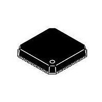
ADP3290JCPZ-RL ON Semiconductor, ADP3290JCPZ-RL Datasheet - Page 28

ADP3290JCPZ-RL
Manufacturer Part Number
ADP3290JCPZ-RL
Description
IC CTLR BUCK SW REG 40-LFCSP
Manufacturer
ON Semiconductor
Type
Step-Down (Buck)r
Datasheet
1.ADP3290JCPZ-RL.pdf
(30 pages)
Specifications of ADP3290JCPZ-RL
Internal Switch(s)
No
Synchronous Rectifier
Yes
Number Of Outputs
4
Voltage - Output
0.5 ~ 1.6 V
Frequency - Switching
250kHz ~ 4MHz
Voltage - Input
12V
Operating Temperature
0°C ~ 85°C
Mounting Type
Surface Mount
Package / Case
40-LFCSP
Output Voltage
0.5 V to 1.6 V
Output Current
500 uA
Input Voltage
- 0.3 V to + 6.3 V
Supply Current
25 mA
Switching Frequency
450 kHz
Mounting Style
SMD/SMT
Maximum Operating Temperature
+ 85 C
Minimum Operating Temperature
0 C
Lead Free Status / RoHS Status
Lead free / RoHS Compliant
Current - Output
-
Power - Output
-
Lead Free Status / Rohs Status
Lead free / RoHS Compliant
Available stocks
Company
Part Number
Manufacturer
Quantity
Price
inductors to ground), no ripple voltage is present during load
release. Therefore, the user does not have to add headroom
for ripple. This allows load release V
than V
specifications.
droop, this implies that capacitors can be removed. When
removing capacitors, also check the output ripple voltage to
make sure it is still within specifications.
Layout and Component Placement
performance of a switching regulator in a PC system.
General Requirements
recommended. This provides the needed versatility for
control circuitry interconnections with optimal placement,
power planes for ground, input and output power, and wide
Because the ADP3290 turns off all of the phases (switches
If V
The following guidelines are recommended for optimal
For good results, a PCB with at least four layers is
19. If both overshoots are larger than desired, try
20. For load release (see Figure 18), if V
TRAN1
making the adjustments using the following
suggestions:
• Make the ramp resistor larger by 25% (R
• For V
frequency
• For V
If these adjustments do not change the response, the
design is limited by the output decoupling. Check
the output response every time a change is made, and
check the switching nodes to ensure that the
response is still stable.
larger than the allowed overshoot, there is not
enough output capacitance. Either more
capacitance is needed, or the inductor values need
to be made smaller. When changing inductors,
start the design again using a spreadsheet and this
tuning procedure.
TRAN1
Figure 18. Transient Setting Waveform
V
and V
TRANREL
TRAN1
TRAN2
by the amount of ripple, and still meet
TRANREL
, increase C
, increase R
are less than the desired final
B
A
or increase the switching
and decrease C
TRANREL
V
DROOP
TRANREL
to be larger
A
RAMP
by 25%
http://onsemi.com
is
)
28
interconnection traces in the remainder of the power
delivery current paths. Keep in mind that each square unit of
1 ounce copper trace has a resistance of ~0.53 mW at room
temperature.
layers, use vias liberally to create several parallel current
paths, so the resistance and inductance introduced by these
current paths is minimized and the via current rating is not
exceeded.
lines of the ADP3290) must cross through power circuitry,
it is best to interpose a signal ground plane between those
signal lines and the traces of the power circuitry. This serves
as a shield to minimize noise injection into the signals at the
expense of making signal ground a bit noisier.
the ADP3290 as a reference for the components associated
with the controller. This plane should be tied to the nearest
output decoupling capacitor ground and should not be tied
to any other power circuitry to prevent power currents from
flowing into it.
close to the controller with short traces. The most important
traces to keep short and away from other traces are the FB
pin and CSSUM pin. The output capacitors should be
connected as close as possible to the load (or connector), for
example, a microprocessor core, that receives the power. If
the load is distributed, the capacitors should also be
distributed and generally be in proportion to where the load
tends to be more dynamic.
path loop described in the Power Circuitry Recommendations
sections.
Power Circuitry Recommendations
encompass the shortest possible length to minimize radiated
switching noise energy (EMI) and conduction losses in the
board. Failure to take proper precautions often results in
EMI problems for the entire PC system and noise−related
operational problems in the power converter control
circuitry. The switching power path is the loop formed by
the current path through the input capacitors and the power
MOSFETs, including all interconnecting PCB traces and
planes. Using short and wide interconnection traces is
especially critical in this path for two reasons: it minimizes
the inductance in the switching loop, which can cause high
energy ringing; and it accommodates the high current
demand with minimal voltage loss.
power MOSFET, is soldered to a PCB, it is recommended to
liberally use the vias, both directly on the mounting pad and
immediately surrounding it. Two important reasons for this
are improved current rating through the vias and improved
thermal performance from vias extended to the opposite side
of the PCB, where a plane can more readily transfer the heat
Whenever high currents must be routed between PCB
If critical signal lines (including the output voltage sense
An analog ground plane should be used around and under
The components around the ADP3290 should be located
Avoid crossing any signal lines over the switching power
The switching power path should be routed on the PCB to
When a power dissipating component, for example, a


