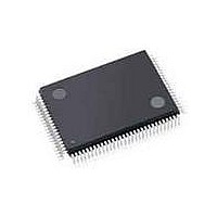
C8051F020-TB Silicon Laboratories Inc, C8051F020-TB Datasheet - Page 60

C8051F020-TB
Manufacturer Part Number
C8051F020-TB
Description
BOARD PROTOTYPING W/C8051F020
Manufacturer
Silicon Laboratories Inc
Type
MCUr
Specifications of C8051F020-TB
Contents
Board
Processor To Be Evaluated
C8051F02x
Interface Type
USB
Lead Free Status / RoHS Status
Contains lead / RoHS non-compliant
For Use With/related Products
C8051F020
Lead Free Status / Rohs Status
Lead free / RoHS Compliant
- Current page: 60 of 272
- Download datasheet (2Mb)
C8051F022/3
The Temperature Sensor transfer function is shown in Figure 6.2. The output voltage (V
the Temperature Sensor is selected by bits AMX0AD3-0 in register AMX0SL; this voltage will be amplified by the
PGA according to the user-programmed PGA settings.
6.2.
ADC0 has a maximum conversion speed of 100 ksps. The ADC0 conversion clock is derived from the system clock
divided by the value held in the ADCSC bits of register ADC0CF.
6.2.1. Starting a Conversion
A conversion can be initiated in one of four ways, depending on the programmed states of the ADC0 Start of Conver-
sion Mode bits (AD0CM1, AD0CM0) in ADC0CN. Conversions may be initiated by:
The AD0BUSY bit is set to logic 1 during conversion and restored to logic 0 when conversion is complete. The fall-
ing edge of AD0BUSY triggers an interrupt (when enabled) and sets the AD0INT interrupt flag (ADC0CN.5). Con-
verted data is available in the ADC0 data word MSB and LSB registers, ADC0H, ADC0L. Converted data can be
either left or right justified in the ADC0H:ADC0L register pair (see example in Figure 6.11) depending on the pro-
grammed state of the AD0LJST bit in the ADC0CN register.
When initiating conversions by writing a ‘1’ to AD0BUSY, the AD0INT bit should be polled to determine when a
conversion has completed (ADC0 interrupts may also be used). The recommended polling procedure is shown below.
60
ADC Modes of Operation
1.
2.
3.
4.
Step 1. Write a ‘0’ to AD0INT;
Step 2. Write a ‘1’ to AD0BUSY;
Step 3. Poll AD0INT for ‘1’;
Step 4. Process ADC0 data.
Writing a ‘1’ to the AD0BUSY bit of ADC0CN;
A Timer 3 overflow (i.e. timed continuous conversions);
A rising edge detected on the external ADC convert start signal, CNVSTR;
A Timer 2 overflow (i.e. timed continuous conversions).
1.000
0.900
0.800
0.700
0.600
0.500
(Volts)
Figure 6.2. Temperature Sensor Transfer Function
-50
0
Rev. 1.4
V
TEMP
50
= 0.00286(TEMP
for PGA Gain = 1
100
C
) + 0.776
(Celsius)
TEMP
) is the PGA input when
Related parts for C8051F020-TB
Image
Part Number
Description
Manufacturer
Datasheet
Request
R
Part Number:
Description:
SMD/C°/SINGLE-ENDED OUTPUT SILICON OSCILLATOR
Manufacturer:
Silicon Laboratories Inc
Part Number:
Description:
Manufacturer:
Silicon Laboratories Inc
Datasheet:
Part Number:
Description:
N/A N/A/SI4010 AES KEYFOB DEMO WITH LCD RX
Manufacturer:
Silicon Laboratories Inc
Datasheet:
Part Number:
Description:
N/A N/A/SI4010 SIMPLIFIED KEY FOB DEMO WITH LED RX
Manufacturer:
Silicon Laboratories Inc
Datasheet:
Part Number:
Description:
N/A/-40 TO 85 OC/EZLINK MODULE; F930/4432 HIGH BAND (REV E/B1)
Manufacturer:
Silicon Laboratories Inc
Part Number:
Description:
EZLink Module; F930/4432 Low Band (rev e/B1)
Manufacturer:
Silicon Laboratories Inc
Part Number:
Description:
I°/4460 10 DBM RADIO TEST CARD 434 MHZ
Manufacturer:
Silicon Laboratories Inc
Part Number:
Description:
I°/4461 14 DBM RADIO TEST CARD 868 MHZ
Manufacturer:
Silicon Laboratories Inc
Part Number:
Description:
I°/4463 20 DBM RFSWITCH RADIO TEST CARD 460 MHZ
Manufacturer:
Silicon Laboratories Inc
Part Number:
Description:
I°/4463 20 DBM RADIO TEST CARD 868 MHZ
Manufacturer:
Silicon Laboratories Inc
Part Number:
Description:
I°/4463 27 DBM RADIO TEST CARD 868 MHZ
Manufacturer:
Silicon Laboratories Inc
Part Number:
Description:
I°/4463 SKYWORKS 30 DBM RADIO TEST CARD 915 MHZ
Manufacturer:
Silicon Laboratories Inc
Part Number:
Description:
N/A N/A/-40 TO 85 OC/4463 RFMD 30 DBM RADIO TEST CARD 915 MHZ
Manufacturer:
Silicon Laboratories Inc
Part Number:
Description:
I°/4463 20 DBM RADIO TEST CARD 169 MHZ
Manufacturer:
Silicon Laboratories Inc


