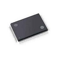
C8051F020-TB Silicon Laboratories Inc, C8051F020-TB Datasheet - Page 94

C8051F020-TB
Manufacturer Part Number
C8051F020-TB
Description
BOARD PROTOTYPING W/C8051F020
Manufacturer
Silicon Laboratories Inc
Type
MCUr
Specifications of C8051F020-TB
Contents
Board
Processor To Be Evaluated
C8051F02x
Interface Type
USB
Lead Free Status / RoHS Status
Contains lead / RoHS non-compliant
For Use With/related Products
C8051F020
Lead Free Status / Rohs Status
Lead free / RoHS Compliant
- Current page: 94 of 272
- Download datasheet (2Mb)
C8051F020/1/2/3
The temperature sensor connects to the highest order input of the ADC0 input multiplexer (see
Multiplexer and PGA” on page 43
page 59
While disabled, the temperature sensor defaults to a high impedance state and any A/D measurements performed on
the sensor while disabled result in undefined data.
94
VDD = 3.0 V, AV+ = 3.0 V, -40°C to +85°C unless otherwise specified
INTERNAL REFERENCE (REFBE = 1)
Output Voltage
VREF Short-Circuit Current
VREF Temperature Coefficient
Load Regulation
VREF Turn-on Time 1
VREF Turn-on Time 2
VREF Turn-on Time 3
EXTERNAL REFERENCE (REFBE = 0)
Input Voltage Range
Input Current
Bits7-5:
Bit4:
Bit3:
Bit2:
Bit1:
Bit0:
R/W
Bit7
-
for C8051F022/3 devices). The TEMPE bit within REF0CN enables and disables the temperature sensor.
PARAMETER
UNUSED. Read = 000b; Write = don’t care.
AD0VRS: ADC0 Voltage Reference Select
0: ADC0 voltage reference from VREFA pin.
1: ADC0 voltage reference from DAC0 output.
AD1VRS: ADC1 Voltage Reference Select
0: ADC1 voltage reference from VREFA pin.
1: ADC1 voltage reference from AV+.
TEMPE: Temperature Sensor Enable Bit.
0: Internal Temperature Sensor Off.
1: Internal Temperature Sensor On.
BIASE: ADC/DAC Bias Generator Enable Bit. (Must be ‘1’ if using ADC or DAC).
0: Internal Bias Generator Off.
1: Internal Bias Generator On.
REFBE: Internal Reference Buffer Enable Bit.
0: Internal Reference Buffer Off.
1: Internal Reference Buffer On. Internal voltage reference is driven on the VREF pin.
R/W
Bit6
-
Table 10.1. Voltage Reference Electrical Characteristics
Figure 10.2. REF0CN: Reference Control Register
R/W
Bit5
-
25°C ambient
Load = 0 to 200 µA to AGND
4.7µF tantalum, 0.1µF ceramic bypass
0.1µF ceramic bypass
no bypass cap
for C8051F020/1 devices, or
AD0VRS
R/W
Bit4
CONDITIONS
AD1VRS
Rev. 1.4
R/W
Bit3
Section “6.1. Analog Multiplexer and PGA” on
TEMPE
R/W
Bit2
MIN
2.36
1.00
BIASE
R/W
Bit1
TYP
2.43
0.5
15
20
10
2
0
REFBE
R/W
Bit0
(AV+) -
Section “5.1. Analog
MAX
2.48
30
0.3
1
SFR Address:
00000000
Reset Value
0xD1
ppm/µA
UNITS
ppm/°C
mA
µA
ms
µs
µs
V
V
Related parts for C8051F020-TB
Image
Part Number
Description
Manufacturer
Datasheet
Request
R
Part Number:
Description:
SMD/C°/SINGLE-ENDED OUTPUT SILICON OSCILLATOR
Manufacturer:
Silicon Laboratories Inc
Part Number:
Description:
Manufacturer:
Silicon Laboratories Inc
Datasheet:
Part Number:
Description:
N/A N/A/SI4010 AES KEYFOB DEMO WITH LCD RX
Manufacturer:
Silicon Laboratories Inc
Datasheet:
Part Number:
Description:
N/A N/A/SI4010 SIMPLIFIED KEY FOB DEMO WITH LED RX
Manufacturer:
Silicon Laboratories Inc
Datasheet:
Part Number:
Description:
N/A/-40 TO 85 OC/EZLINK MODULE; F930/4432 HIGH BAND (REV E/B1)
Manufacturer:
Silicon Laboratories Inc
Part Number:
Description:
EZLink Module; F930/4432 Low Band (rev e/B1)
Manufacturer:
Silicon Laboratories Inc
Part Number:
Description:
I°/4460 10 DBM RADIO TEST CARD 434 MHZ
Manufacturer:
Silicon Laboratories Inc
Part Number:
Description:
I°/4461 14 DBM RADIO TEST CARD 868 MHZ
Manufacturer:
Silicon Laboratories Inc
Part Number:
Description:
I°/4463 20 DBM RFSWITCH RADIO TEST CARD 460 MHZ
Manufacturer:
Silicon Laboratories Inc
Part Number:
Description:
I°/4463 20 DBM RADIO TEST CARD 868 MHZ
Manufacturer:
Silicon Laboratories Inc
Part Number:
Description:
I°/4463 27 DBM RADIO TEST CARD 868 MHZ
Manufacturer:
Silicon Laboratories Inc
Part Number:
Description:
I°/4463 SKYWORKS 30 DBM RADIO TEST CARD 915 MHZ
Manufacturer:
Silicon Laboratories Inc
Part Number:
Description:
N/A N/A/-40 TO 85 OC/4463 RFMD 30 DBM RADIO TEST CARD 915 MHZ
Manufacturer:
Silicon Laboratories Inc
Part Number:
Description:
I°/4463 20 DBM RADIO TEST CARD 169 MHZ
Manufacturer:
Silicon Laboratories Inc


