AD9517-2/PCBZ Analog Devices Inc, AD9517-2/PCBZ Datasheet - Page 11
AD9517-2/PCBZ
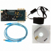
Manufacturer Part Number
AD9517-2/PCBZ
Description
BOARD EVAL FOR AD9517-2
Manufacturer
Analog Devices Inc
Datasheet
1.AD9517-2ABCPZ-RL7.pdf
(80 pages)
Specifications of AD9517-2/PCBZ
Main Purpose
Timing, Clock Generator
Embedded
No
Utilized Ic / Part
AD9517-2
Primary Attributes
2 Inputs, 12 Outputs, 2.2GHz VCO
Secondary Attributes
CMOS, LVDS, LVPECL Output Logic, ADIsimCLK™ Graphical User Interface
Lead Free Status / RoHS Status
Lead free / RoHS Compliant


CLOCK OUTPUT ADDITIVE TIME JITTER (VCO DIVIDER NOT USED)
Table 11.
Parameter
LVPECL OUTPUT ADDITIVE TIME JITTER
LVDS OUTPUT ADDITIVE TIME JITTER
CMOS OUTPUT ADDITIVE TIME JITTER
CLOCK OUTPUT ADDITIVE TIME JITTER (VCO DIVIDER USED)
Table 12.
Parameter
LVPECL OUTPUT ADDITIVE TIME JITTER
LVDS OUTPUT ADDITIVE TIME JITTER
CMOS OUTPUT ADDITIVE TIME JITTER
CLK = 622.08 MHz; LVPECL = 622.08 MHz; Divider = 1
CLK = 622.08 MHz; LVPECL = 155.52 MHz; Divider = 4
CLK = 1.6 GHz; LVPECL = 100 MHz; Divider = 16
CLK = 500 MHz; LVPECL = 100 MHz; Divider = 5
CLK = 1.6 GHz; LVDS = 800 MHz; Divider = 2;
CLK = 1 GHz; LVDS = 200 MHz; Divider = 5
CLK = 1.6 GHz; LVDS = 100 MHz; Divider = 16
CLK = 1.6 GHz; CMOS = 100 MHz; Divider = 16
CLK = 2.4 GHz; VCO DIV = 2; LVPECL = 100 MHz;
CLK = 2.4 GHz; VCO DIV = 2; LVDS = 100 MHz;
CLK = 2.4 GHz; VCO DIV = 2; CMOS = 100 MHz;
VCO Divider Not Used
Divider = 12; Duty-Cycle Correction = Off
Divider = 12; Duty-Cycle Correction = Off
Divider = 12; Duty-Cycle Correction = Off
Min
Min
Rev. B | Page 11 of 80
Typ
40
80
215
245
85
113
280
365
Typ
210
285
350
Max
Max
Unit
fs rms
fs rms
fs rms
fs rms
fs rms
fs rms
fs rms
fs rms
Unit
fs rms
fs rms
fs rms
Test Conditions/Comments
Distribution section only; does not include
PLL and VCO; uses rising edge of clock signal
BW = 12 kHz to 20 MHz
BW = 12 kHz to 20 MHz
Calculated from SNR of ADC method;
DCC not used for even divides
Calculated from SNR of ADC method; DCC on
Distribution section only; does not include
PLL and VCO; uses rising edge of clock signal
BW = 12 kHz to 20 MHz
BW = 12 kHz to 20 MHz
Calculated from SNR of ADC method;
DCC not used for even divides
Distribution section only; does not include
PLL and VCO; uses rising edge of clock signal
Calculated from SNR of ADC method;
DCC not used for even divides
Test Conditions/Comments
Distribution section only; does not include
PLL and VCO; uses rising edge of clock signal
Calculated from SNR of ADC method
Distribution section only; does not include
PLL and VCO; uses rising edge of clock signal
Calculated from SNR of ADC method
Distribution section only; does not include
PLL and VCO; uses rising edge of clock signal
Calculated from SNR of ADC method
AD9517-2
Related parts for AD9517-2/PCBZ
Image
Part Number
Description
Manufacturer
Datasheet
Request
R

Part Number:
Description:
BOARD EVAL FOR AD9517-1
Manufacturer:
Analog Devices Inc
Datasheet:

Part Number:
Description:
12-Output Clock Generator With 2.8GHz VC
Manufacturer:
Analog Devices Inc
Datasheet:
Part Number:
Description:
12-Output Clock Generator With 2.8GHz VC
Manufacturer:
Analog Devices Inc
Datasheet:
Part Number:
Description:
12-Output Clock Generator With 2.8GHz VC
Manufacturer:
Analog Devices Inc
Datasheet:
Part Number:
Description:
12-Output Clock Generator With 2.8GHz VC
Manufacturer:
Analog Devices Inc
Datasheet:
Part Number:
Description:
12-Output Clock Generator With 2.8GHz VC
Manufacturer:
Analog Devices Inc
Datasheet:
Part Number:
Description:
12-Output Clock Generator With 2.8GHz VC
Manufacturer:
Analog Devices Inc
Datasheet:
Part Number:
Description:
BOARD EVALUATION AD9517-4
Manufacturer:
Analog Devices Inc
Datasheet:
Part Number:
Description:
12-Output Clock Generator With 2.5GHz VC
Manufacturer:
Analog Devices Inc
Datasheet:
Part Number:
Description:
12OutputClock Generator With 2.0 GHz VCO
Manufacturer:
Analog Devices Inc
Datasheet:
Part Number:
Description:
12OutputClock Generator With 1.8 GHz VCO
Manufacturer:
Analog Devices Inc
Datasheet:

Part Number:
Description:
IC CLOCK GEN 1.8GHZ VCO 48-LFCSP
Manufacturer:
Analog Devices Inc
Datasheet:
Part Number:
Description:
12-Output Clock Generator With 2.8GHz VC
Manufacturer:
Analog Devices Inc
Datasheet:
Part Number:
Description:
12-Output Clock Generator With 2.8GHz VC
Manufacturer:
Analog Devices Inc
Datasheet:
Part Number:
Description:
12-Output Clock Generator With 2.5GHz VC
Manufacturer:
Analog Devices Inc
Datasheet: