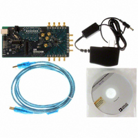
AD9517-2/PCBZ Analog Devices Inc, AD9517-2/PCBZ Datasheet - Page 46

AD9517-2/PCBZ
Manufacturer Part Number
AD9517-2/PCBZ
Description
BOARD EVAL FOR AD9517-2
Manufacturer
Analog Devices Inc
Datasheet
1.AD9517-2ABCPZ-RL7.pdf
(80 pages)
Specifications of AD9517-2/PCBZ
Main Purpose
Timing, Clock Generator
Embedded
No
Utilized Ic / Part
AD9517-2
Primary Attributes
2 Inputs, 12 Outputs, 2.2GHz VCO
Secondary Attributes
CMOS, LVDS, LVPECL Output Logic, ADIsimCLK™ Graphical User Interface
Lead Free Status / RoHS Status
Lead free / RoHS Compliant
AD9517-2
Calculating the Fine Delay
The following values and equations are used to calculate the
delay of the delay block.
Example: 101 = 1 + 1 = 2; 110 = 1 + 1 = 2; 100 = 2 + 1 = 3;
001 = 2 + 1 = 3; 111 = 0 + 1 = 1.
Note that only delay fraction values up to 47 decimal (101111b;
0x2F) are supported.
In no case can the fine delay exceed one-half of the output clock
period. If a delay longer than half of the clock period is attempted,
the output stops clocking.
The delay function adds some jitter greater than that specified
for the nondelayed output. This means that the delay function
should be used primarily for clocking digital chips, such as
FPGA, ASIC, DUC, and DDC. An output with this delay
enabled may not be suitable for clocking data converters. The
jitter is higher for long full scales because the delay block uses a
ramp and trip points to create the variable delay. A slower ramp
time produces more time jitter.
Synchronizing the Outputs—SYNC Function
The AD9517 clock outputs can be synchronized to each other.
Outputs can be individually excluded from synchronization.
Synchronization consists of setting the nonexcluded outputs to
a preset set of static conditions and subsequently releasing these
outputs to continue clocking at the same instant with the preset
conditions applied. This allows for the alignment of the edges of
I
Number of Capacitors = Number of Bits =
0 in Ramp Capacitors + 1
Delay Range (ns) = 200 × ((No. of Caps + 3)/(I
Delay Full Scale (ns) = Delay Range + Offset
Fine Delay (ns) =
Delay Range × Delay Fraction × (1/63) + Offset
Offset
RAMP
(μA) = 200 × (Ramp Current + 1)
( )
ns
=
0.34
+
(
1600
−
I
RAMP
)
×
10
−
4
+
⎛
⎜
⎜
⎝
RAMP
No.
of
)) × 1.3286
I
RAMP
Caps
−
Rev. B | Page 46 of 80
1
⎞
× ⎟ ⎟
⎠
6
two or more outputs or for the spacing of edges according to the
coarse phase offset settings for two or more outputs.
Synchronization of the outputs is executed in several ways:
•
•
•
•
•
•
The most common way to execute the SYNC function is to use
the SYNC pin to do a manual synchronization of the outputs.
This requires a low-going signal on the SYNC pin, which is held
low and then released when synchronization is desired. The
timing of the SYNC operation is shown in
VCO divider) and
an uncertainty of up to one cycle of the clock at the input to the
channel divider due to the asynchronous nature of the SYNC
signal with respect to the clock edges inside the AD9517. The
delay from the
output clocking is between 14 and 15 cycles of clock at the
channel divider input, plus either one cycle of the VCO divider
input (see
(see
Cycles are counted from the rising edge of the signal.
Another common way to execute the SYNC function is by setting
and resetting the soft SYNC bit at Register 0x230[0] (see Table 53
through Table 62 for details). Both setting and resetting of the
soft SYNC bit require an update all registers (Register 0x232[0] = 1)
operation to take effect.
Figure 57
The SYNC pin is forced low and then released (manual sync).
By setting and then resetting any one of the following three
bits: the soft SYNC bit (Register 0x230[0]), the soft reset bit
(Register 0x000[2] [mirrored]), and the distribution power-
down bit (Register 0x230[1]).
Synchronization of the outputs can be executed as part of
the chip power-up sequence.
The RESET pin is forced low and then released (chip reset).
The PD pin is forced low, then released (chip power-down).
When a VCO calibration is completed, an internal SYNC
signal is automatically asserted at the beginning and released
upon the completion of a VCO calibration.
Figure 56
), depending on whether the VCO divider is used.
SYNC rising edge to the beginning of synchronized
Figure 57
), or one cycle of the channel divider input
(VCO divider not used). There is
Figure 56
(using


