AD9517-2/PCBZ Analog Devices Inc, AD9517-2/PCBZ Datasheet - Page 74
AD9517-2/PCBZ
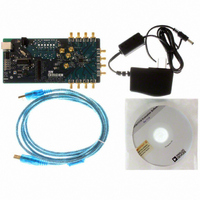
Manufacturer Part Number
AD9517-2/PCBZ
Description
BOARD EVAL FOR AD9517-2
Manufacturer
Analog Devices Inc
Datasheet
1.AD9517-2ABCPZ-RL7.pdf
(80 pages)
Specifications of AD9517-2/PCBZ
Main Purpose
Timing, Clock Generator
Embedded
No
Utilized Ic / Part
AD9517-2
Primary Attributes
2 Inputs, 12 Outputs, 2.2GHz VCO
Secondary Attributes
CMOS, LVDS, LVPECL Output Logic, ADIsimCLK™ Graphical User Interface
Lead Free Status / RoHS Status
Lead free / RoHS Compliant


AD9517-2
Table 60. VCO Divider and CLK Input
Reg.
Addr
(Hex)
0x1E0
0x1E1
0x1E1
Table 61. System
Reg.
Addr.
(Hex)
0x230
Table 62. Update All Registers
Reg.
Addr
(Hex)
0x232
Bits
[2:0]
4
3
2
1
0
Bits
2
1
0
Bits
0
Name
Power down SYNC
Power down distribution reference
Soft SYNC
Name
Update all registers
Name
VCO divider
Power down clock input section
Power down VCO clock interface
Power down VCO and CLK
Select VCO or CLK
Bypass VCO divider
Description
2
0
0
0
0
1
1
1
1
Power down the clock input section (including CLK buffer, VCO divider, and CLK tree).
0: normal operation (default).
1: power-down.
Power down the interface block between VCO and clock distribution.
0: normal operation (default).
1: power-down.
Power down both VCO and CLK input.
0; normal operation (default).
1: power-down.
Select either the VCO or the CLK as the input to VCO divider.
0: select external CLK as input to VCO divider (default).
1: select VCO as input to VCO divider; cannot bypass VCO divider when this is selected.
Bypass or use the VCO divider.
0: use VCO divider (default).
1: bypass VCO divider; cannot select VCO as input when this is selected.
Description
Power down the SYNC function.
0: normal operation of the SYNC function (default).
1: power down SYNC circuitry.
Power down the reference for distribution section.
0: normal operation of the reference for the distribution section (default).
1: power down the reference for the distribution section.
The soft SYNC bit works the same as the SYNC pin, except that the polarity of the bit
is reversed. That is, a high level forces selected channels into a predetermined static
state, and a 1-to-0 transition triggers a SYNC.
0: same as SYNC high (default).
1: same as SYNC low.
Description
This bit must be set to 1 to transfer the contents of the buffer registers into the active
registers, which happens on the next SCLK rising edge. This bit is self-clearing; that is,
it does not have to be set back to 0.
1 (self-clearing): update all active registers to the contents of the buffer registers.
1
0
0
1
1
0
0
1
1
Rev. B | Page 74 of 80
0
0
1
0
1
0
1
0
1
Divide
2.
3.
4 (default).
5.
6.
Output static. Note that setting the VCO divider static should occur only
after VCO calibration.
Output static. Note that setting the VCO divider static should occur only
after VCO calibration.
Output static. Note that setting the VCO divider static should occur only
after VCO calibration.
Related parts for AD9517-2/PCBZ
Image
Part Number
Description
Manufacturer
Datasheet
Request
R

Part Number:
Description:
BOARD EVAL FOR AD9517-1
Manufacturer:
Analog Devices Inc
Datasheet:

Part Number:
Description:
12-Output Clock Generator With 2.8GHz VC
Manufacturer:
Analog Devices Inc
Datasheet:
Part Number:
Description:
12-Output Clock Generator With 2.8GHz VC
Manufacturer:
Analog Devices Inc
Datasheet:
Part Number:
Description:
12-Output Clock Generator With 2.8GHz VC
Manufacturer:
Analog Devices Inc
Datasheet:
Part Number:
Description:
12-Output Clock Generator With 2.8GHz VC
Manufacturer:
Analog Devices Inc
Datasheet:
Part Number:
Description:
12-Output Clock Generator With 2.8GHz VC
Manufacturer:
Analog Devices Inc
Datasheet:
Part Number:
Description:
12-Output Clock Generator With 2.8GHz VC
Manufacturer:
Analog Devices Inc
Datasheet:
Part Number:
Description:
BOARD EVALUATION AD9517-4
Manufacturer:
Analog Devices Inc
Datasheet:
Part Number:
Description:
12-Output Clock Generator With 2.5GHz VC
Manufacturer:
Analog Devices Inc
Datasheet:
Part Number:
Description:
12OutputClock Generator With 2.0 GHz VCO
Manufacturer:
Analog Devices Inc
Datasheet:
Part Number:
Description:
12OutputClock Generator With 1.8 GHz VCO
Manufacturer:
Analog Devices Inc
Datasheet:

Part Number:
Description:
IC CLOCK GEN 1.8GHZ VCO 48-LFCSP
Manufacturer:
Analog Devices Inc
Datasheet:
Part Number:
Description:
12-Output Clock Generator With 2.8GHz VC
Manufacturer:
Analog Devices Inc
Datasheet:
Part Number:
Description:
12-Output Clock Generator With 2.8GHz VC
Manufacturer:
Analog Devices Inc
Datasheet:
Part Number:
Description:
12-Output Clock Generator With 2.5GHz VC
Manufacturer:
Analog Devices Inc
Datasheet: