AD9517-2/PCBZ Analog Devices Inc, AD9517-2/PCBZ Datasheet - Page 14
AD9517-2/PCBZ
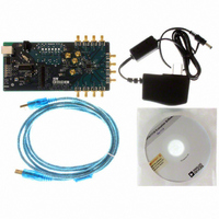
Manufacturer Part Number
AD9517-2/PCBZ
Description
BOARD EVAL FOR AD9517-2
Manufacturer
Analog Devices Inc
Datasheet
1.AD9517-2ABCPZ-RL7.pdf
(80 pages)
Specifications of AD9517-2/PCBZ
Main Purpose
Timing, Clock Generator
Embedded
No
Utilized Ic / Part
AD9517-2
Primary Attributes
2 Inputs, 12 Outputs, 2.2GHz VCO
Secondary Attributes
CMOS, LVDS, LVPECL Output Logic, ADIsimCLK™ Graphical User Interface
Lead Free Status / RoHS Status
Lead free / RoHS Compliant


AD9517-2
POWER DISSIPATION
Table 17.
Parameter
POWER DISSIPATION, CHIP
POWER DELTAS, INDIVIDUAL FUNCTIONS
Power-On Default
Full Operation; CMOS Outputs at 195 MHz
Full Operation; LVDS Outputs at 195 MHz
PD Power-Down
PD Power-Down, Maximum Sleep
V
VCO Divider
REFIN (Differential)
REF1, REF2 (Single-Ended)
VCO
PLL
Channel Divider
LVPECL Channel (Divider Plus Output Driver)
LVPECL Driver
LVDS Channel (Divider Plus Output Driver)
LVDS Driver
CMOS Channel (Divider Plus Output Driver)
CMOS Driver (Second in Pair)
CMOS Driver (First in Second Pair)
Fine Delay Block
CP
Supply
Min
Typ
1.0
1.4
1.4
75
31
4
30
20
4
70
75
30
160
90
120
50
100
0
30
50
Rev. B | Page 14 of 80
Max
1.2
2.0
2.1
185
4.8
Unit
W
W
W
mW
mW
mW
mW
mW
mW
mW
mW
mW
mW
mW
mW
mW
mW
mW
mW
mW
PLL operating; typical closed-loop configuration
Power delta when a function is enabled/disabled
All references off to differential reference enabled
CLK input selected to VCO selected
Test Conditions/Comments
No clock; no programming; default register values;
does not include power dissipated in external resistors
PLL on; internal VCO = 2335 MHz; VCO divider = 2;
all channel dividers on; six LVPECL outputs @ 584 MHz;
eight CMOS outputs (10 pF load) @ 195 MHz; all fine delay
on, maximum current; does not include power dissipated
in external resistors
PLL on; internal VCO = 2335 MHz, VCO divider = 2;
all channel dividers on; six LVPECL outputs @ 584 MHz;
four LVDS outputs @ 195 MHz; all fine delay on, maximum
current; does not include power dissipated in external
resistors
PD pin pulled low; does not include power dissipated
in terminations
PD pin pulled low; PLL power-down Register 0x010[1:0] = 01b;
SYNC power-down, Register 0x230[2] = 1b; REF for distribution
power-down, Register 0x230[1] = 1b
VCO divider not used
All references off to REF1 or REF2 enabled; differential
reference not enabled
PLL off to PLL on, normal operation; no reference enabled
Divider bypassed to divide-by-2 to divide-by-32
No LVPECL output on to one LVPECL output on
Second LVPECL output turned on, same channel
No LVDS output on to one LVDS output on
Second LVDS output turned on, same channel
Static; no CMOS output on to one CMOS output on
Static; second CMOS output, same pair, turned on
Static; first output, second pair, turned on
Delay block off to delay block enabled; maximum current
setting
Related parts for AD9517-2/PCBZ
Image
Part Number
Description
Manufacturer
Datasheet
Request
R

Part Number:
Description:
BOARD EVAL FOR AD9517-1
Manufacturer:
Analog Devices Inc
Datasheet:

Part Number:
Description:
12-Output Clock Generator With 2.8GHz VC
Manufacturer:
Analog Devices Inc
Datasheet:
Part Number:
Description:
12-Output Clock Generator With 2.8GHz VC
Manufacturer:
Analog Devices Inc
Datasheet:
Part Number:
Description:
12-Output Clock Generator With 2.8GHz VC
Manufacturer:
Analog Devices Inc
Datasheet:
Part Number:
Description:
12-Output Clock Generator With 2.8GHz VC
Manufacturer:
Analog Devices Inc
Datasheet:
Part Number:
Description:
12-Output Clock Generator With 2.8GHz VC
Manufacturer:
Analog Devices Inc
Datasheet:
Part Number:
Description:
12-Output Clock Generator With 2.8GHz VC
Manufacturer:
Analog Devices Inc
Datasheet:
Part Number:
Description:
BOARD EVALUATION AD9517-4
Manufacturer:
Analog Devices Inc
Datasheet:
Part Number:
Description:
12-Output Clock Generator With 2.5GHz VC
Manufacturer:
Analog Devices Inc
Datasheet:
Part Number:
Description:
12OutputClock Generator With 2.0 GHz VCO
Manufacturer:
Analog Devices Inc
Datasheet:
Part Number:
Description:
12OutputClock Generator With 1.8 GHz VCO
Manufacturer:
Analog Devices Inc
Datasheet:

Part Number:
Description:
IC CLOCK GEN 1.8GHZ VCO 48-LFCSP
Manufacturer:
Analog Devices Inc
Datasheet:
Part Number:
Description:
12-Output Clock Generator With 2.8GHz VC
Manufacturer:
Analog Devices Inc
Datasheet:
Part Number:
Description:
12-Output Clock Generator With 2.8GHz VC
Manufacturer:
Analog Devices Inc
Datasheet:
Part Number:
Description:
12-Output Clock Generator With 2.5GHz VC
Manufacturer:
Analog Devices Inc
Datasheet: