AD9517-2/PCBZ Analog Devices Inc, AD9517-2/PCBZ Datasheet - Page 51
AD9517-2/PCBZ
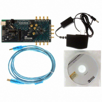
Manufacturer Part Number
AD9517-2/PCBZ
Description
BOARD EVAL FOR AD9517-2
Manufacturer
Analog Devices Inc
Datasheet
1.AD9517-2ABCPZ-RL7.pdf
(80 pages)
Specifications of AD9517-2/PCBZ
Main Purpose
Timing, Clock Generator
Embedded
No
Utilized Ic / Part
AD9517-2
Primary Attributes
2 Inputs, 12 Outputs, 2.2GHz VCO
Secondary Attributes
CMOS, LVDS, LVPECL Output Logic, ADIsimCLK™ Graphical User Interface
Lead Free Status / RoHS Status
Lead free / RoHS Compliant


Read
If the instruction word is for a read operation, the next N × 8
SCLK cycles clock out the data from the address specified in the
instruction word, where N is 1 to 3 as determined by [W1:W0].
If N = 4, the read operation is in streaming mode, continuing
until CS is raised. Streaming mode does not skip over reserved
or blank registers. The readback data is valid on the falling
edge of SCLK.
The default mode of the AD9517 serial control port is the
bidirectional mode. In bidirectional mode, both the sent data
and the readback data appear on the SDIO pin. It is also possible to
set the AD9517 to unidirectional mode via the SDO active bit,
Register 0x000[0] = 1. In unidirectional mode, the readback
data appears on the SDO pin.
A readback request reads the data that is in the serial control
port buffer area, or the data that is in the active registers (see
Figure 62). Readback of the buffer or active registers is controlled
by Register 0x004[0].
The AD9517 supports only the long instruction mode; therefore,
Register 0x000[4:3] must be set to 11b. Long instruction mode is
the default at power-up or reset.
The AD9517 uses Register Address 0x000 to Register
Address 0x232.
THE INSTRUCTION WORD (16 BITS)
The MSB of the instruction word is R/
whether the instruction is a read or a write. The next two bits,
[W1:W0], indicate the length of the transfer in bytes. The final
13 bits are the address ([A12:A0]) at which to begin the read or
write operation.
For a write, the instruction word is followed by the number of
bytes of data indicated by Bits[W1:W0] (see Table 47).
Table 47. Byte Transfer Count
W1
0
0
1
1
Figure 62. Relationship Between Serial Control Port Buffer Registers and
SCLK
SDIO
SDO
CS
W0
0
1
0
1
WRITE REGISTER 0x232 = 0x01
TO UDATE REGISTERS
SERIAL
CONTROL
PORT
Active Registers of the AD9517
Bytes to Transfer
1
2
3
Streaming mode
REGISTERS
UPDATE
W
, which indicates
Rev. B | Page 51 of 80
The 13 bits found in [A12:A0] select the address within the
register map that is written to or read from during the data
transfer portion of the communications cycle. Only Bits[A9:A0]
are needed to cover the range of the 0x232 registers used by the
AD9517. Bits[A12:A10] must always be 0b. For multibyte
transfers, this address is the starting byte address. In MSB first
mode, subsequent bytes increment the address.
MSB/LSB FIRST TRANSFERS
The AD9517 instruction word and byte data can be MSB first
or LSB first. Any data written to Register 0x000 must be mirrored;
the upper four bits (Bits[7:4]) must mirror the lower four bits
(Bits[3:0). This makes it irrelevant whether LSB first or MSB
first is in effect. As an example of this mirroring, see the default
setting for this register: 0x18, which mirrors Bit 4 and Bit 3.
This sets the long instruction mode (which is the default and is
the only mode supported).
The default for the AD9517 is MSB first.
When LSB first is set by Register 0x000[1] and Register 0x000[6],
it takes effect immediately because it affects only the operation
of the serial control port and does not require that an update be
executed.
When MSB first mode is active, the instruction and data bytes
must be written from MSB to LSB. Multibyte data transfers in
MSB first format start with an instruction byte that includes the
register address of the most significant data byte. Subsequent
data bytes must follow in order from the high address to the low
address. In MSB first mode, the serial control port internal
address generator decrements for each data byte of the
multibyte transfer cycle.
When LSB first is active, the instruction and data bytes must be
written from LSB to MSB. Multibyte data transfers in LSB first
format start with an instruction byte that includes the register
address of the least significant data byte followed by multiple
data bytes. The internal byte address generator of the serial
control port increments for each byte of the multibyte
transfer cycle.
The AD9517 serial control port register address decrements
from the register address just written toward 0x000 for multibyte
I/O operations if the MSB first mode is active (default). If the
LSB first mode is active, the register address of the serial control
port increments from the address just written toward 0x232 for
multibyte I/O operations.
Streaming mode always terminates when it hits Address 0x232.
Note that unused addresses are not skipped during multibyte
I/O operations.
Table 48. Streaming Mode (No Addresses Are Skipped)
Write Mode
LSB first
MSB first
Address Direction
Increment
Decrement
Stop Sequence
0x230, 0x231, 0x232, stop
0x001, 0x000, 0x232, stop
AD9517-2
Related parts for AD9517-2/PCBZ
Image
Part Number
Description
Manufacturer
Datasheet
Request
R

Part Number:
Description:
BOARD EVAL FOR AD9517-1
Manufacturer:
Analog Devices Inc
Datasheet:

Part Number:
Description:
12-Output Clock Generator With 2.8GHz VC
Manufacturer:
Analog Devices Inc
Datasheet:
Part Number:
Description:
12-Output Clock Generator With 2.8GHz VC
Manufacturer:
Analog Devices Inc
Datasheet:
Part Number:
Description:
12-Output Clock Generator With 2.8GHz VC
Manufacturer:
Analog Devices Inc
Datasheet:
Part Number:
Description:
12-Output Clock Generator With 2.8GHz VC
Manufacturer:
Analog Devices Inc
Datasheet:
Part Number:
Description:
12-Output Clock Generator With 2.8GHz VC
Manufacturer:
Analog Devices Inc
Datasheet:
Part Number:
Description:
12-Output Clock Generator With 2.8GHz VC
Manufacturer:
Analog Devices Inc
Datasheet:
Part Number:
Description:
BOARD EVALUATION AD9517-4
Manufacturer:
Analog Devices Inc
Datasheet:
Part Number:
Description:
12-Output Clock Generator With 2.5GHz VC
Manufacturer:
Analog Devices Inc
Datasheet:
Part Number:
Description:
12OutputClock Generator With 2.0 GHz VCO
Manufacturer:
Analog Devices Inc
Datasheet:
Part Number:
Description:
12OutputClock Generator With 1.8 GHz VCO
Manufacturer:
Analog Devices Inc
Datasheet:

Part Number:
Description:
IC CLOCK GEN 1.8GHZ VCO 48-LFCSP
Manufacturer:
Analog Devices Inc
Datasheet:
Part Number:
Description:
12-Output Clock Generator With 2.8GHz VC
Manufacturer:
Analog Devices Inc
Datasheet:
Part Number:
Description:
12-Output Clock Generator With 2.8GHz VC
Manufacturer:
Analog Devices Inc
Datasheet:
Part Number:
Description:
12-Output Clock Generator With 2.5GHz VC
Manufacturer:
Analog Devices Inc
Datasheet: