AD9517-2/PCBZ Analog Devices Inc, AD9517-2/PCBZ Datasheet - Page 17
AD9517-2/PCBZ
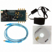
Manufacturer Part Number
AD9517-2/PCBZ
Description
BOARD EVAL FOR AD9517-2
Manufacturer
Analog Devices Inc
Datasheet
1.AD9517-2ABCPZ-RL7.pdf
(80 pages)
Specifications of AD9517-2/PCBZ
Main Purpose
Timing, Clock Generator
Embedded
No
Utilized Ic / Part
AD9517-2
Primary Attributes
2 Inputs, 12 Outputs, 2.2GHz VCO
Secondary Attributes
CMOS, LVDS, LVPECL Output Logic, ADIsimCLK™ Graphical User Interface
Lead Free Status / RoHS Status
Lead free / RoHS Compliant


PIN CONFIGURATION AND FUNCTION DESCRIPTIONS
Table 20. Pin Function Descriptions
Pin No.
1
2
3
4
5
6
7
8
9
10, 24, 25,
30, 31, 36,
37, 43, 45
11
12
13
14
Input/
Output
I
O
I
O
O
I
I
I
O
I
I
I
I
I
Pin Type
3.3 V CMOS
3.3 V CMOS
Power
3.3 V CMOS
3.3 V CMOS
3.3 V CMOS
3.3 V CMOS
Loop filter
Loop filter
Power
Differential
clock input
Differential
clock input
3.3 V CMOS
3.3 V CMOS
REF_SEL
NOTES
1. THE EXTERNAL PADDLE ON THE BOTTOM OF THE PACKAGE MUST BE
Mnemonic
REFMON
LD
VCP
CP
STATUS
REF_SEL
SYNC
LF
BYPASS
VS
CLK
CLK
SCLK
CS
REFMON
BYPASS
STATUS
CONNECTED TO GROUND FOR PROPER OPERATION.
SYNC
VCP
CLK
CLK
LD
CP
VS
LF
10
11
12
1
2
3
4
5
6
7
8
9
PIN 1
INDICATOR
Description
Reference Monitor (Output). This pin has multiple selectable outputs; see Table 54,
Register 0x01B.
Lock Detect (Output). This pin has multiple selectable outputs; see Table 54,
Register 0x01A.
Power Supply for Charge Pump (CP); V
Charge Pump (Output). Connects to external loop filter.
Status (Output). This pin has multiple selectable outputs; see Table 54, Register 0x017.
Reference Select. Selects REF1 (low) or REF2 (high). This pin has an internal 30 kΩ
pull-down resistor.
Manual Synchronizations and Manual Holdover. This pin initiates a manual
synchronization and is also used for manual holdover. Active low. This pin has an
internal 30 kΩ pull-up resistor.
Loop Filter (Input). Connects to VCO control voltage node internally. This pin has
31 pF of internal capacitance to ground, which may influence the loop filter design
for large loop bandwidths.
This pin is for bypassing the LDO to ground with a capacitor.
3.3 V Power Pins.
Along with CLK, this is the self-biased differential input for the clock distribution
section.
Along with CLK, this is the self-biased differential input for the clock distribution
section.
Serial Control Port Data Clock Signal.
Serial Control Port Chip Select; Active Low. This pin has an internal 30 kΩ pull-up
resistor.
Figure 6. Pin Configuration
(Not to Scale)
Rev. B | Page 17 of 80
AD9517-2
TOP VIEW
36
35
34
33
32
31
30
29
28
27
26
25
VS
OUT4 (OUT4A)
OUT4 (OUT4B)
OUT5 (OUT5A)
OUT5 (OUT5B)
VS
OUT7 (OUT7B)
OUT7 (OUT7A)
OUT6 (OUT6B)
OUT6 (OUT6A)
S
≤ V
CP
≤ 5.0 V.
AD9517-2
Related parts for AD9517-2/PCBZ
Image
Part Number
Description
Manufacturer
Datasheet
Request
R

Part Number:
Description:
BOARD EVAL FOR AD9517-1
Manufacturer:
Analog Devices Inc
Datasheet:

Part Number:
Description:
12-Output Clock Generator With 2.8GHz VC
Manufacturer:
Analog Devices Inc
Datasheet:
Part Number:
Description:
12-Output Clock Generator With 2.8GHz VC
Manufacturer:
Analog Devices Inc
Datasheet:
Part Number:
Description:
12-Output Clock Generator With 2.8GHz VC
Manufacturer:
Analog Devices Inc
Datasheet:
Part Number:
Description:
12-Output Clock Generator With 2.8GHz VC
Manufacturer:
Analog Devices Inc
Datasheet:
Part Number:
Description:
12-Output Clock Generator With 2.8GHz VC
Manufacturer:
Analog Devices Inc
Datasheet:
Part Number:
Description:
12-Output Clock Generator With 2.8GHz VC
Manufacturer:
Analog Devices Inc
Datasheet:
Part Number:
Description:
BOARD EVALUATION AD9517-4
Manufacturer:
Analog Devices Inc
Datasheet:
Part Number:
Description:
12-Output Clock Generator With 2.5GHz VC
Manufacturer:
Analog Devices Inc
Datasheet:
Part Number:
Description:
12OutputClock Generator With 2.0 GHz VCO
Manufacturer:
Analog Devices Inc
Datasheet:
Part Number:
Description:
12OutputClock Generator With 1.8 GHz VCO
Manufacturer:
Analog Devices Inc
Datasheet:

Part Number:
Description:
IC CLOCK GEN 1.8GHZ VCO 48-LFCSP
Manufacturer:
Analog Devices Inc
Datasheet:
Part Number:
Description:
12-Output Clock Generator With 2.8GHz VC
Manufacturer:
Analog Devices Inc
Datasheet:
Part Number:
Description:
12-Output Clock Generator With 2.8GHz VC
Manufacturer:
Analog Devices Inc
Datasheet:
Part Number:
Description:
12-Output Clock Generator With 2.5GHz VC
Manufacturer:
Analog Devices Inc
Datasheet: