AD9517-2/PCBZ Analog Devices Inc, AD9517-2/PCBZ Datasheet - Page 53
AD9517-2/PCBZ
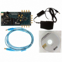
Manufacturer Part Number
AD9517-2/PCBZ
Description
BOARD EVAL FOR AD9517-2
Manufacturer
Analog Devices Inc
Datasheet
1.AD9517-2ABCPZ-RL7.pdf
(80 pages)
Specifications of AD9517-2/PCBZ
Main Purpose
Timing, Clock Generator
Embedded
No
Utilized Ic / Part
AD9517-2
Primary Attributes
2 Inputs, 12 Outputs, 2.2GHz VCO
Secondary Attributes
CMOS, LVDS, LVPECL Output Logic, ADIsimCLK™ Graphical User Interface
Lead Free Status / RoHS Status
Lead free / RoHS Compliant


Table 50. Serial Control Port Timing
Parameter
t
t
t
t
t
t
t
t
DS
DH
CLK
S
C
HIGH
LOW
DV
SCLK
SDIO
CS
Description
Setup time between data and rising edge of SCLK
Hold time between data and rising edge of SCLK
Period of the clock
Setup time between CS falling edge and SCLK rising edge (start of communication cycle)
Setup time between SCLK rising edge and CS rising edge (end of communication cycle)
Minimum period that SCLK should be in a logic high state
Minimum period that SCLK should be in a logic low state
SCLK to valid SDIO and SDO (see Figure 66)
t
t
DS
S
BIT N
t
HIGH
t
DH
Figure 68. Serial Control Port Timing—Write
t
CLK
Rev. B | Page 53 of 80
t
LOW
BIT N + 1
t
C
AD9517-2
Related parts for AD9517-2/PCBZ
Image
Part Number
Description
Manufacturer
Datasheet
Request
R

Part Number:
Description:
BOARD EVAL FOR AD9517-1
Manufacturer:
Analog Devices Inc
Datasheet:

Part Number:
Description:
12-Output Clock Generator With 2.8GHz VC
Manufacturer:
Analog Devices Inc
Datasheet:
Part Number:
Description:
12-Output Clock Generator With 2.8GHz VC
Manufacturer:
Analog Devices Inc
Datasheet:
Part Number:
Description:
12-Output Clock Generator With 2.8GHz VC
Manufacturer:
Analog Devices Inc
Datasheet:
Part Number:
Description:
12-Output Clock Generator With 2.8GHz VC
Manufacturer:
Analog Devices Inc
Datasheet:
Part Number:
Description:
12-Output Clock Generator With 2.8GHz VC
Manufacturer:
Analog Devices Inc
Datasheet:
Part Number:
Description:
12-Output Clock Generator With 2.8GHz VC
Manufacturer:
Analog Devices Inc
Datasheet:
Part Number:
Description:
BOARD EVALUATION AD9517-4
Manufacturer:
Analog Devices Inc
Datasheet:
Part Number:
Description:
12-Output Clock Generator With 2.5GHz VC
Manufacturer:
Analog Devices Inc
Datasheet:
Part Number:
Description:
12OutputClock Generator With 2.0 GHz VCO
Manufacturer:
Analog Devices Inc
Datasheet:
Part Number:
Description:
12OutputClock Generator With 1.8 GHz VCO
Manufacturer:
Analog Devices Inc
Datasheet:

Part Number:
Description:
IC CLOCK GEN 1.8GHZ VCO 48-LFCSP
Manufacturer:
Analog Devices Inc
Datasheet:
Part Number:
Description:
12-Output Clock Generator With 2.8GHz VC
Manufacturer:
Analog Devices Inc
Datasheet:
Part Number:
Description:
12-Output Clock Generator With 2.8GHz VC
Manufacturer:
Analog Devices Inc
Datasheet:
Part Number:
Description:
12-Output Clock Generator With 2.5GHz VC
Manufacturer:
Analog Devices Inc
Datasheet: