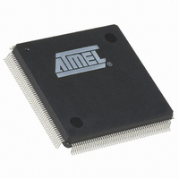
AT91RM9200-QU-002 Atmel, AT91RM9200-QU-002 Datasheet - Page 218

AT91RM9200-QU-002
Manufacturer Part Number
AT91RM9200-QU-002
Description
IC ARM9 MCU 208 PQFP
Manufacturer
Atmel
Series
AT91SAMr
Datasheets
1.AT91RM9200-EK.pdf
(41 pages)
2.AT91RM9200-QU-002.pdf
(701 pages)
3.AT91RM9200-QU-002.pdf
(38 pages)
Specifications of AT91RM9200-QU-002
Core Processor
ARM9
Core Size
16/32-Bit
Speed
180MHz
Connectivity
EBI/EMI, Ethernet, I²C, MMC, SPI, SSC, UART/USART, USB
Peripherals
POR
Number Of I /o
122
Program Memory Size
128KB (128K x 8)
Program Memory Type
ROM
Ram Size
48K x 8
Voltage - Supply (vcc/vdd)
1.65 V ~ 1.95 V
Oscillator Type
Internal
Operating Temperature
-40°C ~ 85°C
Package / Case
208-MQFP, 208-PQFP
Processor Series
AT91Rx
Core
ARM7TDMI
Data Bus Width
32 bit
Data Ram Size
16 KB
Interface Type
2-Wire, EBI, I2S, SPI, UART, USART
Maximum Clock Frequency
180 MHz
Number Of Programmable I/os
122
Number Of Timers
10 bit
Operating Supply Voltage
3 V to 3.6 V
Maximum Operating Temperature
+ 85 C
Mounting Style
SMD/SMT
3rd Party Development Tools
JTRACE-ARM-2M, MDK-ARM, RL-ARM, ULINK2
Development Tools By Supplier
AT91SAM-ICE, AT91-ISP, AT91RM9200-EK
Minimum Operating Temperature
- 40 C
Eeprom Memory
0 Bytes
Input Output
122
Interface
EBI/EMI, UART/USART
Ios
122
Memory Type
ROM
Number Of Bits
32
Package Type
208-pin PQFP
Programmable Memory
128K Bytes
Timers
3-16-bit
Voltage, Range
1.65-1.95 V
Cpu Family
91R
Device Core
ARM920T
Device Core Size
32b
Frequency (max)
180MHz
Total Internal Ram Size
16KB
# I/os (max)
122
Number Of Timers - General Purpose
6
Operating Supply Voltage (typ)
1.8/3.3V
Operating Supply Voltage (max)
1.95/3.6V
Operating Supply Voltage (min)
1.65/3V
Instruction Set Architecture
RISC
Operating Temp Range
-40C to 85C
Operating Temperature Classification
Industrial
Mounting
Surface Mount
Pin Count
208
For Use With
AT91SAM-ICE - EMULATOR FOR AT91 ARM7/ARM9
Lead Free Status / RoHS Status
Lead free / RoHS Compliant
Eeprom Size
-
Data Converters
-
Lead Free Status / Rohs Status
Lead free / RoHS Compliant
Available stocks
Company
Part Number
Manufacturer
Quantity
Price
Company:
Part Number:
AT91RM9200-QU-002
Manufacturer:
COSMO
Quantity:
12 000
Company:
Part Number:
AT91RM9200-QU-002
Manufacturer:
Atmel
Quantity:
1 680
Company:
Part Number:
AT91RM9200-QU-002
Manufacturer:
ATMEL
Quantity:
2 350
Part Number:
AT91RM9200-QU-002
Manufacturer:
ATMEL/爱特梅尔
Quantity:
20 000
Company:
Part Number:
AT91RM9200-QU-002-CQ
Manufacturer:
Atmel
Quantity:
3
- Current page: 218 of 701
- Download datasheet (10Mb)
20.5
20.5.1
20.6
20.6.1
20.6.2
Figure 20-3. Burst Flash Clock Rates
20.6.3
218
BFC Clock
Product Dependencies
Functional Description
AT91RM9200
I/O Lines
Burst Flash Controller Reset State
Burst Flash Controller Clock Selection
Burst Flash Controller Asynchronous Mode
MCK
BFCC = 1
The pins used for interfacing the Burst Flash Controller may be multiplexed with the PIO lines.
The programmer must first program the PIO controller to assign the Burst Flash Controller pins
to their peripheral function. If I/O lines of the Burst Flash Controller are not used by the applica-
tion, they can be used for other purposes by the PIO Controller.
The Burst Flash Controller drives the following signals:
When enabled, the BFC also drives the address bus, the data bus and the Chip Select (BFCS)
line. The Ready Signal (BFRDY) is taken as an input and used as an indicator for the next data
availability.
After reset, the BFC is disabled and, therefore, must be enabled by programming the field
BFCOM.
Controller operates in Asynchronous Mode. The Burst Flash memory can be programmed by
writing and reading in Asynchronous Mode.
The BFC clock rate is programmable to be either Master Clock, Master Clock divided by 2 or
Master Clock divided by 4. The clock selection is necessary in Burst Mode as well as in Asyn-
chronous Mode. The latency fields in the mode register and all burst Flash control signal
waveforms are related to the Burst Flash Clock (BFCK) period.
The BFC clock rate is selected by the BFCC field.
page 227
In Asynchronous Mode, the Burst Flash Controller clock is off. The BFCK signal is driven low.
The BFC performs read access to bytes (8-bits), half-words (16-bits), and words (32-bits). In the
last case, the BFC autonomously transforms the word read request into two separate half-word
reads. This is fully transparent to the user.
• Address Valid (BFAVD), to latch the addresses
• Clock (BFCK), to supply the burst clock
• Burst Advance Address (BFBAA), to control the Burst Flash memory address advance when
• Write Enable (BFWE), to write to the Burst Flash device
• Output Enable (BFOE), to enable the external device data drive on the data bus
programmed to operate in signal controlled burst advance
BFC Clock
See “Burst Flash Controller Mode Register” on page 227.
MCK
BFCC = 2
BFC Clock
MCK
“Burst Flash Controller Mode Register” on
BFCC = 3
At this time, the Burst Flash
1768I–ATARM–09-Jul-09
Related parts for AT91RM9200-QU-002
Image
Part Number
Description
Manufacturer
Datasheet
Request
R

Part Number:
Description:
Manufacturer:
ATMEL Corporation
Datasheet:

Part Number:
Description:
IC ARM MCU 16BIT 128K 256BGA
Manufacturer:
Atmel
Datasheet:

Part Number:
Description:
IC ARM9 MCU 208 PQFP
Manufacturer:
Atmel
Datasheet:

Part Number:
Description:
DEVEL KIT
Manufacturer:
Atmel
Datasheet:

Part Number:
Description:
KIT DEVELOPMENT AT91RM9200
Manufacturer:
Atmel
Datasheet:

Part Number:
Description:
IC ARM9 MCU 256 BGA
Manufacturer:
Atmel
Datasheet:

Part Number:
Description:
IC ARM MCU 16BIT 128K 208PQFP
Manufacturer:
Atmel
Datasheet:

Part Number:
Description:
AT91RM9200 Development Kit
Manufacturer:
ATMEL Corporation
Datasheet:

Part Number:
Description:
DEV KIT FOR AVR/AVR32
Manufacturer:
Atmel
Datasheet:

Part Number:
Description:
INTERVAL AND WIPE/WASH WIPER CONTROL IC WITH DELAY
Manufacturer:
ATMEL Corporation
Datasheet:

Part Number:
Description:
Low-Voltage Voice-Switched IC for Hands-Free Operation
Manufacturer:
ATMEL Corporation
Datasheet:

Part Number:
Description:
MONOLITHIC INTEGRATED FEATUREPHONE CIRCUIT
Manufacturer:
ATMEL Corporation
Datasheet:

Part Number:
Description:
AM-FM Receiver IC U4255BM-M
Manufacturer:
ATMEL Corporation
Datasheet:


