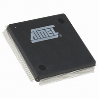
AT91RM9200-QU-002 Atmel, AT91RM9200-QU-002 Datasheet - Page 326

AT91RM9200-QU-002
Manufacturer Part Number
AT91RM9200-QU-002
Description
IC ARM9 MCU 208 PQFP
Manufacturer
Atmel
Series
AT91SAMr
Datasheets
1.AT91RM9200-EK.pdf
(41 pages)
2.AT91RM9200-QU-002.pdf
(701 pages)
3.AT91RM9200-QU-002.pdf
(38 pages)
Specifications of AT91RM9200-QU-002
Core Processor
ARM9
Core Size
16/32-Bit
Speed
180MHz
Connectivity
EBI/EMI, Ethernet, I²C, MMC, SPI, SSC, UART/USART, USB
Peripherals
POR
Number Of I /o
122
Program Memory Size
128KB (128K x 8)
Program Memory Type
ROM
Ram Size
48K x 8
Voltage - Supply (vcc/vdd)
1.65 V ~ 1.95 V
Oscillator Type
Internal
Operating Temperature
-40°C ~ 85°C
Package / Case
208-MQFP, 208-PQFP
Processor Series
AT91Rx
Core
ARM7TDMI
Data Bus Width
32 bit
Data Ram Size
16 KB
Interface Type
2-Wire, EBI, I2S, SPI, UART, USART
Maximum Clock Frequency
180 MHz
Number Of Programmable I/os
122
Number Of Timers
10 bit
Operating Supply Voltage
3 V to 3.6 V
Maximum Operating Temperature
+ 85 C
Mounting Style
SMD/SMT
3rd Party Development Tools
JTRACE-ARM-2M, MDK-ARM, RL-ARM, ULINK2
Development Tools By Supplier
AT91SAM-ICE, AT91-ISP, AT91RM9200-EK
Minimum Operating Temperature
- 40 C
Eeprom Memory
0 Bytes
Input Output
122
Interface
EBI/EMI, UART/USART
Ios
122
Memory Type
ROM
Number Of Bits
32
Package Type
208-pin PQFP
Programmable Memory
128K Bytes
Timers
3-16-bit
Voltage, Range
1.65-1.95 V
Cpu Family
91R
Device Core
ARM920T
Device Core Size
32b
Frequency (max)
180MHz
Total Internal Ram Size
16KB
# I/os (max)
122
Number Of Timers - General Purpose
6
Operating Supply Voltage (typ)
1.8/3.3V
Operating Supply Voltage (max)
1.95/3.6V
Operating Supply Voltage (min)
1.65/3V
Instruction Set Architecture
RISC
Operating Temp Range
-40C to 85C
Operating Temperature Classification
Industrial
Mounting
Surface Mount
Pin Count
208
For Use With
AT91SAM-ICE - EMULATOR FOR AT91 ARM7/ARM9
Lead Free Status / RoHS Status
Lead free / RoHS Compliant
Eeprom Size
-
Data Converters
-
Lead Free Status / Rohs Status
Lead free / RoHS Compliant
Available stocks
Company
Part Number
Manufacturer
Quantity
Price
Company:
Part Number:
AT91RM9200-QU-002
Manufacturer:
COSMO
Quantity:
12 000
Company:
Part Number:
AT91RM9200-QU-002
Manufacturer:
Atmel
Quantity:
1 680
Company:
Part Number:
AT91RM9200-QU-002
Manufacturer:
ATMEL
Quantity:
2 350
Part Number:
AT91RM9200-QU-002
Manufacturer:
ATMEL/爱特梅尔
Quantity:
20 000
Company:
Part Number:
AT91RM9200-QU-002-CQ
Manufacturer:
Atmel
Quantity:
3
- Current page: 326 of 701
- Download datasheet (10Mb)
26.4.2.6
26.4.3
26.4.3.1
26.4.3.2
326
AT91RM9200
Transmitter
Receiver Framing Error
Transmitter Reset, Enable and Disable
Transmit Format
bit. If different, the parity error bit PARE in DBGU_SR is set at the same time the RXRDY is set.
The parity bit is cleared when the control register DBGU_CR is written with the bit RSTSTA
(Reset Status) at 1. If a new character is received before the reset status command is written,
the PARE bit remains at 1.
Figure 26-8. Parity Error
When a start bit is detected, it generates a character reception when all the data bits have been
sampled. The stop bit is also sampled and when it is detected at 0, the FRAME (Framing Error)
bit in DBGU_SR is set at the same time the RXRDY bit is set. The bit FRAME remains high until
the control register DBGU_CR is written with the bit RSTSTA at 1.
Figure 26-9. Receiver Framing Error
After device reset, the Debug Unit transmitter is disabled and it must be enabled before being
used. The transmitter is enabled by writing the control register DBGU_CR with the bit TXEN at 1.
From this command, the transmitter waits for a character to be written in the Transmit Holding
Register DBGU_THR before actually starting the transmission.
The programmer can disable the transmitter by writing DBGU_CR with the bit TXDIS at 1. If the
transmitter is not operating, it is immediately stopped. However, if a character is being pro-
cessed into the Shift Register and/or a character has been written in the Transmit Holding
Register, the characters are completed before the transmitter is actually stopped.
The programmer can also put the transmitter in its reset state by writing the DBGU_CR with the
bit RSTTX at 1. This immediately stops the transmitter, whether or not it is processing
characters.
The Debug Unit transmitter drives the pin DTXD at the baud rate clock speed. The line is driven
depending on the format defined in the Mode Register and the data stored in the Shift Register.
One start bit at level 0, then the 8 data bits, from the lowest to the highest bit, one optional parity
bit and one stop bit at 1 are consecutively shifted out as shown on the following figure. The field
RXRDY
PARE
FRAME
DRXD
RXRDY
DRXD
S
S
D0
D0
D1
D1
D2
D2
D3
D3
D4
D4
D5
D5
D6
D6
Wrong Parity Bit
D7
D7
P
P
Detected at 0
Stop Bit
stop
stop
RSTSTA
RSTSTA
1768I–ATARM–09-Jul-09
Related parts for AT91RM9200-QU-002
Image
Part Number
Description
Manufacturer
Datasheet
Request
R

Part Number:
Description:
Manufacturer:
ATMEL Corporation
Datasheet:

Part Number:
Description:
IC ARM MCU 16BIT 128K 256BGA
Manufacturer:
Atmel
Datasheet:

Part Number:
Description:
IC ARM9 MCU 208 PQFP
Manufacturer:
Atmel
Datasheet:

Part Number:
Description:
DEVEL KIT
Manufacturer:
Atmel
Datasheet:

Part Number:
Description:
KIT DEVELOPMENT AT91RM9200
Manufacturer:
Atmel
Datasheet:

Part Number:
Description:
IC ARM9 MCU 256 BGA
Manufacturer:
Atmel
Datasheet:

Part Number:
Description:
IC ARM MCU 16BIT 128K 208PQFP
Manufacturer:
Atmel
Datasheet:

Part Number:
Description:
AT91RM9200 Development Kit
Manufacturer:
ATMEL Corporation
Datasheet:

Part Number:
Description:
DEV KIT FOR AVR/AVR32
Manufacturer:
Atmel
Datasheet:

Part Number:
Description:
INTERVAL AND WIPE/WASH WIPER CONTROL IC WITH DELAY
Manufacturer:
ATMEL Corporation
Datasheet:

Part Number:
Description:
Low-Voltage Voice-Switched IC for Hands-Free Operation
Manufacturer:
ATMEL Corporation
Datasheet:

Part Number:
Description:
MONOLITHIC INTEGRATED FEATUREPHONE CIRCUIT
Manufacturer:
ATMEL Corporation
Datasheet:

Part Number:
Description:
AM-FM Receiver IC U4255BM-M
Manufacturer:
ATMEL Corporation
Datasheet:


