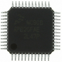
MC908AP32CFAE Freescale Semiconductor, MC908AP32CFAE Datasheet - Page 126

MC908AP32CFAE
Manufacturer Part Number
MC908AP32CFAE
Description
IC MCU 32K FLASH 8MHZ 48-LQFP
Manufacturer
Freescale Semiconductor
Series
HC08r
Specifications of MC908AP32CFAE
Core Processor
HC08
Core Size
8-Bit
Speed
8MHz
Connectivity
I²C, IRSCI, SCI, SPI
Peripherals
LED, LVD, POR, PWM
Number Of I /o
32
Program Memory Size
32KB (32K x 8)
Program Memory Type
FLASH
Ram Size
2K x 8
Voltage - Supply (vcc/vdd)
2.7 V ~ 5.5 V
Data Converters
A/D 8x10b
Oscillator Type
Internal
Operating Temperature
-40°C ~ 85°C
Package / Case
48-LQFP
Controller Family/series
HC08
No. Of I/o's
32
Ram Memory Size
2KB
Cpu Speed
8MHz
No. Of Timers
2
Embedded Interface Type
I2C, SCI, SPI
Rohs Compliant
Yes
Lead Free Status / RoHS Status
Lead free / RoHS Compliant
Eeprom Size
-
Available stocks
Company
Part Number
Manufacturer
Quantity
Price
Company:
Part Number:
MC908AP32CFAE
Manufacturer:
Freescale Semiconductor
Quantity:
10 000
Company:
Part Number:
MC908AP32CFAER
Manufacturer:
Freescale Semiconductor
Quantity:
10 000
- Current page: 126 of 324
- Download datasheet (4Mb)
Monitor ROM (MON)
Upon power-on reset, if the received bytes of the security code do not match the data at locations
$FFF6–$FFFD, the host fails to bypass the security feature. The MCU remains in monitor mode, but
reading a FLASH location returns an invalid value and trying to execute code from FLASH causes an
illegal address reset. After receiving the eight security bytes from the host, the MCU transmits a break
character, signifying that it is ready to receive a command.
To determine whether the security code entered is correct, check to see if bit 6 of RAM address $60 is
set. If it is, then the correct security code has been entered and FLASH can be accessed.
If the security sequence fails, the device should be reset by a power-on reset and brought up in monitor
mode to attempt another entry. After failing the security sequence, the FLASH module can also be mass
erased by executing an erase routine that was downloaded into internal RAM. The mass erase operation
clears the security code locations so that all eight security bytes become $FF (blank).
8.5 ROM-Resident Routines
Seven routines stored in the monitor ROM area (thus ROM-resident) are provided for FLASH memory
manipulation. Five of the seven routines are intended to simplify FLASH program, erase, and load
operations. The other two routines are intended to simplify the use of the FLASH memory as EEPROM.
Table 8-10
The routines are designed to be called as stand-alone subroutines in the user program or monitor mode.
The parameters that are passed to a routine are in the form of a contiguous data block, stored in RAM.
The index register (H:X) is loaded with the address of the first byte of the data block (acting as a pointer),
and the subroutine is called (JSR). Using the start address as a pointer, multiple data blocks can be used,
any area of RAM be used. A data block has the control and data bytes in a defined order, as shown in
Figure
126
8-9.
shows a summary of the ROM-resident routines.
MON_PRGRNGE
MON_ERARNGE
Routine Name
PRGRNGE
ERARNGE
EE_WRITE
EE_READ
The MCU does not transmit a break character until after the host sends the
eight security bits.
LDRNGE
Table 8-10. Summary of ROM-Resident Routines
Program a range of locations
Erase a page or the entire array
Loads data from a range of locations
Program a range of locations in monitor
mode
Erase a page or the entire array in
monitor mode
Emulated EEPROM write. Data size
ranges from 7 to 15 bytes at a time.
Emulated EEPROM read. Data size
ranges from 7 to 15 bytes at a time.
MC68HC908AP Family Data Sheet, Rev. 4
Routine Description
NOTE
Call Address
$FF36
$FD5B
$FCE4
$FC34
$FC00
$FF24
$FF28
Freescale Semiconductor
Stack Used
(bytes)
30
18
15
17
11
9
7
Related parts for MC908AP32CFAE
Image
Part Number
Description
Manufacturer
Datasheet
Request
R
Part Number:
Description:
Manufacturer:
Freescale Semiconductor, Inc
Datasheet:
Part Number:
Description:
Manufacturer:
Freescale Semiconductor, Inc
Datasheet:
Part Number:
Description:
Manufacturer:
Freescale Semiconductor, Inc
Datasheet:
Part Number:
Description:
Manufacturer:
Freescale Semiconductor, Inc
Datasheet:
Part Number:
Description:
Manufacturer:
Freescale Semiconductor, Inc
Datasheet:
Part Number:
Description:
Manufacturer:
Freescale Semiconductor, Inc
Datasheet:
Part Number:
Description:
Manufacturer:
Freescale Semiconductor, Inc
Datasheet:
Part Number:
Description:
Manufacturer:
Freescale Semiconductor, Inc
Datasheet:
Part Number:
Description:
Manufacturer:
Freescale Semiconductor, Inc
Datasheet:
Part Number:
Description:
Manufacturer:
Freescale Semiconductor, Inc
Datasheet:
Part Number:
Description:
Manufacturer:
Freescale Semiconductor, Inc
Datasheet:
Part Number:
Description:
Manufacturer:
Freescale Semiconductor, Inc
Datasheet:
Part Number:
Description:
Manufacturer:
Freescale Semiconductor, Inc
Datasheet:
Part Number:
Description:
Manufacturer:
Freescale Semiconductor, Inc
Datasheet:
Part Number:
Description:
Manufacturer:
Freescale Semiconductor, Inc
Datasheet:


