MC908AP32CFAE Freescale Semiconductor, MC908AP32CFAE Datasheet - Page 182
MC908AP32CFAE
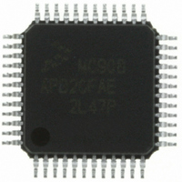
Manufacturer Part Number
MC908AP32CFAE
Description
IC MCU 32K FLASH 8MHZ 48-LQFP
Manufacturer
Freescale Semiconductor
Series
HC08r
Specifications of MC908AP32CFAE
Core Processor
HC08
Core Size
8-Bit
Speed
8MHz
Connectivity
I²C, IRSCI, SCI, SPI
Peripherals
LED, LVD, POR, PWM
Number Of I /o
32
Program Memory Size
32KB (32K x 8)
Program Memory Type
FLASH
Ram Size
2K x 8
Voltage - Supply (vcc/vdd)
2.7 V ~ 5.5 V
Data Converters
A/D 8x10b
Oscillator Type
Internal
Operating Temperature
-40°C ~ 85°C
Package / Case
48-LQFP
Controller Family/series
HC08
No. Of I/o's
32
Ram Memory Size
2KB
Cpu Speed
8MHz
No. Of Timers
2
Embedded Interface Type
I2C, SCI, SPI
Rohs Compliant
Yes
Lead Free Status / RoHS Status
Lead free / RoHS Compliant
Eeprom Size
-
Available stocks
Company
Part Number
Manufacturer
Quantity
Price
Company:

Part Number:
MC908AP32CFAE
Manufacturer:
Freescale Semiconductor
Quantity:
10 000
Company:
Part Number:
MC908AP32CFAER
Manufacturer:
Freescale Semiconductor
Quantity:
10 000


Infrared Serial Communications Interface Module (IRSCI)
12.2 Pin Name Conventions
The generic names of the IRSCI I/O pins are:
IRSCI I/O (input/output) lines are implemented by sharing parallel I/O port pins. The full name of an IRSCI
input or output reflects the name of the shared port pin.
names of the IRSCI I/O pins. The generic pin names appear in the text of this section.
182
$0040
$0041
$0042
$0043
$0044
$0045
$0046
$0047
Addr.
•
•
RxD (receive data)
TxD (transmit data)
IRSCI Baud Rate Register
IRSCI Control Register 1
IRSCI Control Register 2
IRSCI Control Register 3
IRSCI Status Register 1
IRSCI Status Register 2
Register Name
IRSCI Infrared Control
IRSCI Data Register
When the IRSCI is enabled, the SCTxD pin is an open-drain output and
requires a pullup resistor to be connected for proper SCI operation.
(IRSCIRCR)
(IRSCDR)
(IRSCBR)
(IRSCC1)
(IRSCC2)
(IRSCC3)
(IRSCS1)
(IRSCS2)
Register
Generic Pin Names:
Full Pin Names:
Reset:
Reset:
Reset:
Reset:
Reset:
Reset:
Reset:
Reset:
Read:
Read:
Read:
Read:
Read:
Read:
Read:
Read:
Write:
Write:
Write:
Write:
Write:
Write:
Write:
Write:
Figure 12-1. IRSCI I/O Registers Summary
Table 12-1. Pin Name Conventions
MC68HC908AP Family Data Sheet, Rev. 4
LOOPS
SCTIE
SCTE
Bit 7
CKS
R8
R7
T7
U
R
0
0
1
0
0
0
= Unimplemented
ENSCI
TCIE
TC
R6
T8
T6
U
6
0
0
1
0
0
0
0
0
NOTE
DMARE
SCRIE
SCRF
SCP1
R5
T5
5
0
0
0
0
0
0
0
0
0
Table 12-1
PTC7/SCRxD
R = Reserved
RxD
DMATE
Unaffected by reset
SCP0
IDLE
ILIE
R4
T4
M
4
0
0
0
0
0
0
0
0
shows the full names and the generic
WAKE
ORIE
OR
TE
R3
T3
R
R
3
0
0
0
0
0
0
0
PTC6/SCTxD
U = Unaffected
SCR2
TxD
TNP1
NEIE
ILTY
RE
NF
R2
T2
2
0
0
0
0
0
0
0
Freescale Semiconductor
SCR1
TNP0
RWU
FEIE
PEN
BKF
FE
R1
T1
1
0
0
0
0
0
0
0
SCR0
PEIE
IREN
Bit 0
PTY
SBK
RPF
PE
R0
T0
0
0
0
0
0
0
0
Related parts for MC908AP32CFAE
Image
Part Number
Description
Manufacturer
Datasheet
Request
R

Part Number:
Description:
Manufacturer:
Freescale Semiconductor, Inc
Datasheet:
Part Number:
Description:
Manufacturer:
Freescale Semiconductor, Inc
Datasheet:
Part Number:
Description:
Manufacturer:
Freescale Semiconductor, Inc
Datasheet:
Part Number:
Description:
Manufacturer:
Freescale Semiconductor, Inc
Datasheet:
Part Number:
Description:
Manufacturer:
Freescale Semiconductor, Inc
Datasheet:
Part Number:
Description:
Manufacturer:
Freescale Semiconductor, Inc
Datasheet:
Part Number:
Description:
Manufacturer:
Freescale Semiconductor, Inc
Datasheet:
Part Number:
Description:
Manufacturer:
Freescale Semiconductor, Inc
Datasheet:
Part Number:
Description:
Manufacturer:
Freescale Semiconductor, Inc
Datasheet:
Part Number:
Description:
Manufacturer:
Freescale Semiconductor, Inc
Datasheet:
Part Number:
Description:
Manufacturer:
Freescale Semiconductor, Inc
Datasheet:
Part Number:
Description:
Manufacturer:
Freescale Semiconductor, Inc
Datasheet:
Part Number:
Description:
Manufacturer:
Freescale Semiconductor, Inc
Datasheet:
Part Number:
Description:
Manufacturer:
Freescale Semiconductor, Inc
Datasheet:
Part Number:
Description:
Manufacturer:
Freescale Semiconductor, Inc
Datasheet: