MC908AP32CFAE Freescale Semiconductor, MC908AP32CFAE Datasheet - Page 291
MC908AP32CFAE
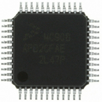
Manufacturer Part Number
MC908AP32CFAE
Description
IC MCU 32K FLASH 8MHZ 48-LQFP
Manufacturer
Freescale Semiconductor
Series
HC08r
Specifications of MC908AP32CFAE
Core Processor
HC08
Core Size
8-Bit
Speed
8MHz
Connectivity
I²C, IRSCI, SCI, SPI
Peripherals
LED, LVD, POR, PWM
Number Of I /o
32
Program Memory Size
32KB (32K x 8)
Program Memory Type
FLASH
Ram Size
2K x 8
Voltage - Supply (vcc/vdd)
2.7 V ~ 5.5 V
Data Converters
A/D 8x10b
Oscillator Type
Internal
Operating Temperature
-40°C ~ 85°C
Package / Case
48-LQFP
Controller Family/series
HC08
No. Of I/o's
32
Ram Memory Size
2KB
Cpu Speed
8MHz
No. Of Timers
2
Embedded Interface Type
I2C, SCI, SPI
Rohs Compliant
Yes
Lead Free Status / RoHS Status
Lead free / RoHS Compliant
Eeprom Size
-
Available stocks
Company
Part Number
Manufacturer
Quantity
Price
Company:

Part Number:
MC908AP32CFAE
Manufacturer:
Freescale Semiconductor
Quantity:
10 000
Company:
Part Number:
MC908AP32CFAER
Manufacturer:
Freescale Semiconductor
Quantity:
10 000


20.3.4 Forced Reset Operation
In applications that require V
module to reset the MCU when V
and LVIRSTD bits must be at logic 0 to enable the LVI module and to enable LVI resets.
20.3.5 Voltage Hysteresis Protection
Once the LVI has triggered (by having V
V
continually entering and exiting reset if V
V
20.4 LVI Status Register
The LVI status register (LVISR) indicates if the V
was detected below V
LVIOUT — LVI Output Bit
20.5 LVI Interrupts
The LVI module does not generate interrupt requests.
Freescale Semiconductor
DD
TRIPF1
This read-only flag becomes set when the V
clears the LVIOUT bit.
rises above the rising trip point voltage, V
by the hysteresis voltage, V
Address:
Reset:
Read:
Write:
LVIOUT
TRIPF2
$FE0F
Bit 7
0
V
.
V
DD
TRIPF2
TRIPF1
= Unimplemented
to remain above the V
V
DD
V
V
V
6
0
0
REG
DD
MC68HC908AP Family Data Sheet, Rev. 4
DD
DD
V
Table 20-1. LVIOUT Bit Indication
Figure 20-3. LVI Status Register
< V
< V
DD
falls below the V
HYS
> V
< V
< V
and
> V
, V
or
or
REG
DD
TRIPR1
TRIPF1
TRIPF2
DD
REG
.
TRIPR2
DD
< V
< V
5
0
0
fall below V
TRIPR1
TRIPR2
is approximately equal to V
DD
TRIPR1
DD
or V
voltage was detected below V
4
0
0
TRIPF1
. This prevents a condition in which the MCU is
REG
TRIPF1
TRIPF1
falls below their respective trip voltages. Reset
level. In the CONFIG1 register, the LVIPWRD
Previous value
), the LVI will maintain a reset condition until
3
0
0
level, enabling LVI resets allows the LVI
LVIOUT
0
1
2
0
0
TRIPF1
. V
1
0
0
TRIPR1
TRIPF1
LVI Status Register
Bit 0
is greater than
or V
0
0
REG
voltage
289
Related parts for MC908AP32CFAE
Image
Part Number
Description
Manufacturer
Datasheet
Request
R

Part Number:
Description:
Manufacturer:
Freescale Semiconductor, Inc
Datasheet:
Part Number:
Description:
Manufacturer:
Freescale Semiconductor, Inc
Datasheet:
Part Number:
Description:
Manufacturer:
Freescale Semiconductor, Inc
Datasheet:
Part Number:
Description:
Manufacturer:
Freescale Semiconductor, Inc
Datasheet:
Part Number:
Description:
Manufacturer:
Freescale Semiconductor, Inc
Datasheet:
Part Number:
Description:
Manufacturer:
Freescale Semiconductor, Inc
Datasheet:
Part Number:
Description:
Manufacturer:
Freescale Semiconductor, Inc
Datasheet:
Part Number:
Description:
Manufacturer:
Freescale Semiconductor, Inc
Datasheet:
Part Number:
Description:
Manufacturer:
Freescale Semiconductor, Inc
Datasheet:
Part Number:
Description:
Manufacturer:
Freescale Semiconductor, Inc
Datasheet:
Part Number:
Description:
Manufacturer:
Freescale Semiconductor, Inc
Datasheet:
Part Number:
Description:
Manufacturer:
Freescale Semiconductor, Inc
Datasheet:
Part Number:
Description:
Manufacturer:
Freescale Semiconductor, Inc
Datasheet:
Part Number:
Description:
Manufacturer:
Freescale Semiconductor, Inc
Datasheet:
Part Number:
Description:
Manufacturer:
Freescale Semiconductor, Inc
Datasheet: