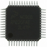
MC908AP32CFAE Freescale Semiconductor, MC908AP32CFAE Datasheet - Page 263

MC908AP32CFAE
Manufacturer Part Number
MC908AP32CFAE
Description
IC MCU 32K FLASH 8MHZ 48-LQFP
Manufacturer
Freescale Semiconductor
Series
HC08r
Specifications of MC908AP32CFAE
Core Processor
HC08
Core Size
8-Bit
Speed
8MHz
Connectivity
I²C, IRSCI, SCI, SPI
Peripherals
LED, LVD, POR, PWM
Number Of I /o
32
Program Memory Size
32KB (32K x 8)
Program Memory Type
FLASH
Ram Size
2K x 8
Voltage - Supply (vcc/vdd)
2.7 V ~ 5.5 V
Data Converters
A/D 8x10b
Oscillator Type
Internal
Operating Temperature
-40°C ~ 85°C
Package / Case
48-LQFP
Controller Family/series
HC08
No. Of I/o's
32
Ram Memory Size
2KB
Cpu Speed
8MHz
No. Of Timers
2
Embedded Interface Type
I2C, SCI, SPI
Rohs Compliant
Yes
Lead Free Status / RoHS Status
Lead free / RoHS Compliant
Eeprom Size
-
Available stocks
Company
Part Number
Manufacturer
Quantity
Price
Company:
Part Number:
MC908AP32CFAE
Manufacturer:
Freescale Semiconductor
Quantity:
10 000
Company:
Part Number:
MC908AP32CFAER
Manufacturer:
Freescale Semiconductor
Quantity:
10 000
- Current page: 263 of 324
- Download datasheet (4Mb)
16.2 Port A
Port A is an 8-bit special-function port that shares all of its pins with the analog-to-digital converter (ADC)
module. Port A pins also have LED direct drive capability.
16.2.1 Port A Data Register (PTA)
The port A data register contains a data latch for each of the eight port A pins.
PTA[7:0] — Port A Data Bits
ADC7–ADC0 — ADC Channels 7 to 0
LED drive — Direct LED drive pins
16.2.2 Data Direction Register (DDRA)
Data direction register A determines whether each port A pin is an input or an output. Writing a logic 1 to
a DDRA bit enables the output buffer for the corresponding port A pin; a logic 0 disables the output buffer.
Freescale Semiconductor
These read/write bits are software-programmable. Data direction of each port A pin is under the control
of the corresponding bit in data direction register A. Reset has no effect on port A data.
ADC7–ADC0 are pins used for the input channels to the analog-to-digital converter module. The
channel select bits, ADCH[4:0], in the ADC status and control register define which port pin will be used
as an ADC input and overrides any control from the port I/O logic.
PTA7–PTA0 pins can be configured for direct LED drive. See
(LEDA).
Alternative Function:
Additional Function: LED drive
Address:
Care must be taken when reading port A while applying analog voltages to
ADC7–ADC0 pins. If the appropriate ADC channel is not enabled,
excessive current drain may occur if analog voltages are applied to the
PTAx/ADCx pin, while PTA is read as a digital input. Those ports not
selected as analog input channels are considered digital I/O ports.
Reset:
Read:
Write:
Address:
Reset:
Read:
Write:
DDRA7
$0004
Bit 7
0
Figure 16-3. Data Direction Register A (DDRA)
$0000
ADC7
PTA7
Bit 7
Figure 16-2. Port A Data Register (PTA)
DDRA6
6
0
MC68HC908AP Family Data Sheet, Rev. 4
LED drive
ADC6
PTA6
6
DDRA5
5
0
LED drive
ADC5
PTA5
5
NOTE
DDRA4
4
0
LED drive
Unaffected by reset
ADC4
PTA4
4
DDRA3
3
0
LED drive
ADC3
PTA3
3
16.2.3 Port-A LED Control Register
DDRA2
2
0
LED drive
ADC2
PTA2
2
DDRA1
1
0
LED drive
ADC1
PTA1
1
DDRA0
Bit 0
0
LED drive
ADC0
PTA0
Bit 0
Port A
261
Related parts for MC908AP32CFAE
Image
Part Number
Description
Manufacturer
Datasheet
Request
R
Part Number:
Description:
Manufacturer:
Freescale Semiconductor, Inc
Datasheet:
Part Number:
Description:
Manufacturer:
Freescale Semiconductor, Inc
Datasheet:
Part Number:
Description:
Manufacturer:
Freescale Semiconductor, Inc
Datasheet:
Part Number:
Description:
Manufacturer:
Freescale Semiconductor, Inc
Datasheet:
Part Number:
Description:
Manufacturer:
Freescale Semiconductor, Inc
Datasheet:
Part Number:
Description:
Manufacturer:
Freescale Semiconductor, Inc
Datasheet:
Part Number:
Description:
Manufacturer:
Freescale Semiconductor, Inc
Datasheet:
Part Number:
Description:
Manufacturer:
Freescale Semiconductor, Inc
Datasheet:
Part Number:
Description:
Manufacturer:
Freescale Semiconductor, Inc
Datasheet:
Part Number:
Description:
Manufacturer:
Freescale Semiconductor, Inc
Datasheet:
Part Number:
Description:
Manufacturer:
Freescale Semiconductor, Inc
Datasheet:
Part Number:
Description:
Manufacturer:
Freescale Semiconductor, Inc
Datasheet:
Part Number:
Description:
Manufacturer:
Freescale Semiconductor, Inc
Datasheet:
Part Number:
Description:
Manufacturer:
Freescale Semiconductor, Inc
Datasheet:
Part Number:
Description:
Manufacturer:
Freescale Semiconductor, Inc
Datasheet:


