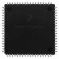
MC9S12HZ128CAL Freescale Semiconductor, MC9S12HZ128CAL Datasheet - Page 270

MC9S12HZ128CAL
Manufacturer Part Number
MC9S12HZ128CAL
Description
IC MCU 16BIT 128K FLASH 112-LQFP
Manufacturer
Freescale Semiconductor
Series
HCS12r
Datasheet
1.MC9S12HZ128CAL.pdf
(692 pages)
Specifications of MC9S12HZ128CAL
Core Processor
HCS12
Core Size
16-Bit
Speed
25MHz
Connectivity
CAN, EBI/EMI, I²C, SCI, SPI
Peripherals
LCD, Motor control PWM, POR, PWM, WDT
Number Of I /o
85
Program Memory Size
128KB (128K x 8)
Program Memory Type
FLASH
Eeprom Size
2K x 8
Ram Size
6K x 8
Voltage - Supply (vcc/vdd)
2.35 V ~ 5.5 V
Data Converters
A/D 16x10b
Oscillator Type
Internal
Operating Temperature
-40°C ~ 85°C
Package / Case
112-LQFP
Processor Series
S12H
Core
HCS12
Data Bus Width
16 bit
Data Ram Size
6 KB
Interface Type
I2C, SCI, SPI
Maximum Clock Frequency
50 MHz
Number Of Programmable I/os
85
Number Of Timers
8
Maximum Operating Temperature
+ 85 C
Mounting Style
SMD/SMT
3rd Party Development Tools
EWHCS12
Minimum Operating Temperature
- 40 C
On-chip Adc
10 bit, 16 Channel
Lead Free Status / RoHS Status
Lead free / RoHS Compliant
Available stocks
Company
Part Number
Manufacturer
Quantity
Price
Company:
Part Number:
MC9S12HZ128CAL
Manufacturer:
Freescale Semiconductor
Quantity:
10 000
- Current page: 270 of 692
- Download datasheet (4Mb)
Chapter 9 Motor Controller (MC10B8CV1)
Whenever FAST = 1, the bits D10, D9, D1, and D0 will be set to 0 if the duty cycle register is written.
For example setting MCDCx = 0x0158 with FAST = 0 gives the same output waveform as setting
MCDCx = 0x5600 with FAST = 1 (with FAST = 1, the low byte of MCDCx needs not to be written).
The state of the FAST bit has impact only during write and read operations. A change of the FAST bit (set
or clear) without writing a new value does not impact the internal interpretation of the duty cycle values.
To prevent the output from inconsistent signals, the duty cycle registers are double buffered. The motor
controller module will use working registers to generate the output signals. The working registers are
copied from the bus accessible registers at the following conditions:
In this way, the output of the PWM will always be either the old PWM waveform or the new PWM
waveform, not some variation in between.
Reads of this register return the most recent value written. Reads do not necessarily return the value of the
currently active sign, duty cycle, and dither functionality due to the double buffering scheme.
1. Odd duty cycle register: MCDCx+1, x = 2 n
270
Field
•
•
•
•
S
0
MCPER is set to 0 (all channels are disabled in this case)
MCAM[1:0] of the respective channel is set to 0 (channel is disabled)
A PWM timer counter overflow occurs while in half H-bridge or full H-bridge mode
A PWM channel pair is configured to work in Dual Full H-Bridge mode and a PWM timer counter
overflow occurs after the odd
SIGN — The SIGN bit is used to define which output will drive the PWM signal in (dual) full-H-bridge modes. The
SIGN bit has no effect in half-bridge modes. See
detailed information about the impact of RECIRC and SIGN bit on the PWM output.
Table 9-9. MCDCx Field Descriptions
MC9S12HZ256 Data Sheet, Rev. 2.05
1
duty cycle register of the channel pair has been written.
Description
Section 9.4.1.3.2, “Sign Bit
(S)”, and table
Freescale Semiconductor
Table 9-11
for
Related parts for MC9S12HZ128CAL
Image
Part Number
Description
Manufacturer
Datasheet
Request
R
Part Number:
Description:
Manufacturer:
Freescale Semiconductor, Inc
Datasheet:
Part Number:
Description:
Manufacturer:
Freescale Semiconductor, Inc
Datasheet:
Part Number:
Description:
Manufacturer:
Freescale Semiconductor, Inc
Datasheet:
Part Number:
Description:
Manufacturer:
Freescale Semiconductor, Inc
Datasheet:
Part Number:
Description:
Manufacturer:
Freescale Semiconductor, Inc
Datasheet:
Part Number:
Description:
Manufacturer:
Freescale Semiconductor, Inc
Datasheet:
Part Number:
Description:
Manufacturer:
Freescale Semiconductor, Inc
Datasheet:
Part Number:
Description:
Manufacturer:
Freescale Semiconductor, Inc
Datasheet:
Part Number:
Description:
Manufacturer:
Freescale Semiconductor, Inc
Datasheet:
Part Number:
Description:
Manufacturer:
Freescale Semiconductor, Inc
Datasheet:
Part Number:
Description:
Manufacturer:
Freescale Semiconductor, Inc
Datasheet:
Part Number:
Description:
Manufacturer:
Freescale Semiconductor, Inc
Datasheet:
Part Number:
Description:
Manufacturer:
Freescale Semiconductor, Inc
Datasheet:
Part Number:
Description:
Manufacturer:
Freescale Semiconductor, Inc
Datasheet:
Part Number:
Description:
Manufacturer:
Freescale Semiconductor, Inc
Datasheet:


