M30833FJGP#U3 Renesas Electronics America, M30833FJGP#U3 Datasheet - Page 142
M30833FJGP#U3
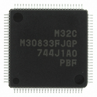
Manufacturer Part Number
M30833FJGP#U3
Description
IC M32C/83 MCU FLASH 100LQFP
Manufacturer
Renesas Electronics America
Series
M16C™ M32C/80r
Datasheets
1.M3087BFLGPU3.pdf
(364 pages)
2.M30833FJGPU3.pdf
(96 pages)
3.M30833FJGPU3.pdf
(529 pages)
Specifications of M30833FJGP#U3
Core Processor
M32C/80
Core Size
16/32-Bit
Speed
32MHz
Connectivity
CAN, I²C, IEBus, SIO, UART/USART
Peripherals
DMA, WDT
Number Of I /o
85
Program Memory Size
512KB (512K x 8)
Program Memory Type
FLASH
Ram Size
31K x 8
Voltage - Supply (vcc/vdd)
3 V ~ 5.5 V
Data Converters
A/D 26x10b; D/A 2x8b
Oscillator Type
Internal
Operating Temperature
-40°C ~ 85°C
Package / Case
100-LQFP
Package
100LQFP
Family Name
R8C
Maximum Speed
32 MHz
Operating Supply Voltage
5 V
Data Bus Width
16 Bit
Number Of Programmable I/os
87
Interface Type
UART
On-chip Adc
26-chx10-bit
On-chip Dac
2-chx8-bit
Number Of Timers
11
For Use With
R0K330879S001BE - KIT DEV RSK M32C/87R0K330879S000BE - KIT DEV RSK M32C/87
Lead Free Status / RoHS Status
Lead free / RoHS Compliant
Eeprom Size
-
Available stocks
Company
Part Number
Manufacturer
Quantity
Price


R
R
M
e
E
3
. v
J
NOTES:
Table 12.2 DMiSL Register (i = 0 to 3) Function
2
0
1
C
9
1. If the INT3 pin is used as data bus in the memory expansion mode or microprocessor mode, a DMA3 interrupt
2. The falling edge and both edges of input signal into the INTj pin (j = 0 to 3) cause a DMA request. The INT interrupt
3. The UkSMR register and UkSMR2 register (k = 0 to 4) switch the UARTj receive to ACK or ACK to UARTk receive.
4. The same setting is used to generate an intelligent I/O interrupt 9 request and a CAN interrupt 0 request.
5. The same setting is used to generate an intelligent I/O interrupt 10 request and a CAN interrupt 1 request.
6. The same setting is used to generate an intelligent I/O interrupt 11 request and a CAN interrupt 2 request.
3 .
b4 b3 b2 b1 b0
B
Setting Value
0 0 0 0 0
0 0 0 0 1
0 0 0 1 0
0 0 0 1 1
0 0 1 0 0
0 0 1 0 1
0 0 1 1 0
0 0 1 1 1
0 1 0 0 0
0 1 0 0 1
0 1 0 1 0
0 1 0 1 1
0 1 1 0 0
0 1 1 0 1
0 1 1 1 0
0 1 1 1 1
1 0 0 0 0
1 0 0 0 1
1 0 0 1 0
1 0 0 1 1
1 0 1 0 0
1 0 1 0 1
1 0 1 1 0
1 0 1 1 1
1 1 0 0 0
1 1 0 0 1
1 1 0 1 0
1 1 0 1 1
1 1 1 0 0
1 1 1 0 1
1 1 1 1 0
1 1 1 1 1
8 /
0
1
request cannot be generated by an input signal to the INT3 pin.
(the POL bit in the INTjlC register, the LVS bit, the IFSR register) is not affected and vice versa.
3
0
3
J
G
4
a
0 -
n
o r
3 .
1
u
, 1
3
p
1
2
(
M
0
0
3
A/D0 Interrupt Request
6
Falling edge of INT0
Both edges of INT0
2
Interrupt 0 Request
Interrupt 1 Request
Interrupt 2 Request
Interrupt 3 Request
Interrupt 4 Request
Interrupt 5 Request
Interrupt 6 Request
C
Intelligent I/O
Intelligent I/O
Intelligent I/O
Intelligent I/O
Intelligent I/O
Intelligent I/O
Intelligent I/O
8 /
Page 117
, 3
DMA0
M
3
2
C
f o
8 /
4
3
8
) T
UART0 Receive or ACK Interrupt Request
UART1 Receive or ACK Interrupt Request
UART2 Receive or ACK Interrupt Request
UART3 Receive or ACK Interrupt Request
UART4 Receive or ACK Interrupt Request
8
A/D1 Interrupt Request
Falling edge of INT1
Interrupt 10 Request
Both edges of INT1
Interrupt 11 Request
Interrupt 9 Request
Interrupt 7 Request
Interrupt 8 Request
Interrupt 0 Request
Interrupt 1 Request
DMA Request Cause
UART0 Transmit Interrupt Request
UART1 Transmit Interrupt Request
UART2 Transmit Interrupt Request
UART3 Transmit Interrupt Request
UART4 Transmit Interrupt Request
Intelligent I/O
Intelligent I/O
Intelligent I/O
Intelligent I/O
Intelligent I/O
Intelligent I/O
Intelligent I/O
DMA1
Timer B0 Interrupt Request
Timer B1 Interrupt Request
Timer B2 Interrupt Request
Timer B3 Interrupt Request
Timer B4 Interrupt Request
Timer B5 Interrupt Request
Timer A0 Interrupt Request
Timer A1 Interrupt Request
Timer A2 Interrupt Request
Timer A3 Interrupt Request
Timer A4 Interrupt Request
Software Trigger
(4)
(6)
(5)
Falling edge of INT2
A/D0 Interrupt request
Both edges of INT2
Interrupt 2 Request
Interrupt 3 Request
Interrupt 4 Request
Interrupt 5 Request
Interrupt 6 Request
Interrupt 7 Request
Interrupt 8 Request
Intelligent I/O
Intelligent I/O
Intelligent I/O
Intelligent I/O
Intelligent I/O
Intelligent I/O
Intelligent I/O
DMA2
(3)
(3)
(3)
(3)
(3)
A/D1 Interrupt Request
Interrupt 10 Request
Interrupt 11 Request
Interrupt 9 Request
Interrupt 0 Request
Interrupt 1 Request
Interrupt 2 Request
Interrupt 3 Request
Intelligent I/O
Intelligent I/O
Intelligent I/O
Intelligent I/O
Intelligent I/O
Intelligent I/O
Intelligent I/O
Falling edge of INT3
Both edges of INT3
DMA3
(4)
(6)
(5)
(1)
(1)
(Note 2)
(Note 2)
12. DMAC
Related parts for M30833FJGP#U3
Image
Part Number
Description
Manufacturer
Datasheet
Request
R

Part Number:
Description:
KIT STARTER FOR M16C/29
Manufacturer:
Renesas Electronics America
Datasheet:

Part Number:
Description:
KIT STARTER FOR R8C/2D
Manufacturer:
Renesas Electronics America
Datasheet:

Part Number:
Description:
R0K33062P STARTER KIT
Manufacturer:
Renesas Electronics America
Datasheet:

Part Number:
Description:
KIT STARTER FOR R8C/23 E8A
Manufacturer:
Renesas Electronics America
Datasheet:

Part Number:
Description:
KIT STARTER FOR R8C/25
Manufacturer:
Renesas Electronics America
Datasheet:

Part Number:
Description:
KIT STARTER H8S2456 SHARPE DSPLY
Manufacturer:
Renesas Electronics America
Datasheet:

Part Number:
Description:
KIT STARTER FOR R8C38C
Manufacturer:
Renesas Electronics America
Datasheet:

Part Number:
Description:
KIT STARTER FOR R8C35C
Manufacturer:
Renesas Electronics America
Datasheet:

Part Number:
Description:
KIT STARTER FOR R8CL3AC+LCD APPS
Manufacturer:
Renesas Electronics America
Datasheet:
Part Number:
Description:
KIT STARTER FOR RX610
Manufacturer:
Renesas Electronics America
Datasheet:

Part Number:
Description:
KIT STARTER FOR R32C/118
Manufacturer:
Renesas Electronics America
Datasheet:

Part Number:
Description:
KIT DEV RSK-R8C/26-29
Manufacturer:
Renesas Electronics America
Datasheet:

Part Number:
Description:
KIT STARTER FOR SH7124
Manufacturer:
Renesas Electronics America
Datasheet:

Part Number:
Description:
KIT STARTER FOR H8SX/1622
Manufacturer:
Renesas Electronics America
Datasheet:

Part Number:
Description:
KIT DEV FOR SH7203
Manufacturer:
Renesas Electronics America
Datasheet: