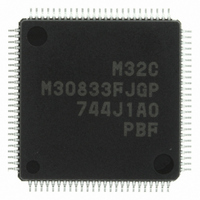
M30833FJGP#U3 Renesas Electronics America, M30833FJGP#U3 Datasheet - Page 356

M30833FJGP#U3
Manufacturer Part Number
M30833FJGP#U3
Description
IC M32C/83 MCU FLASH 100LQFP
Manufacturer
Renesas Electronics America
Series
M16C™ M32C/80r
Datasheets
1.M3087BFLGPU3.pdf
(364 pages)
2.M30833FJGPU3.pdf
(96 pages)
3.M30833FJGPU3.pdf
(529 pages)
Specifications of M30833FJGP#U3
Core Processor
M32C/80
Core Size
16/32-Bit
Speed
32MHz
Connectivity
CAN, I²C, IEBus, SIO, UART/USART
Peripherals
DMA, WDT
Number Of I /o
85
Program Memory Size
512KB (512K x 8)
Program Memory Type
FLASH
Ram Size
31K x 8
Voltage - Supply (vcc/vdd)
3 V ~ 5.5 V
Data Converters
A/D 26x10b; D/A 2x8b
Oscillator Type
Internal
Operating Temperature
-40°C ~ 85°C
Package / Case
100-LQFP
Package
100LQFP
Family Name
R8C
Maximum Speed
32 MHz
Operating Supply Voltage
5 V
Data Bus Width
16 Bit
Number Of Programmable I/os
87
Interface Type
UART
On-chip Adc
26-chx10-bit
On-chip Dac
2-chx8-bit
Number Of Timers
11
For Use With
R0K330879S001BE - KIT DEV RSK M32C/87R0K330879S000BE - KIT DEV RSK M32C/87
Lead Free Status / RoHS Status
Lead free / RoHS Compliant
Eeprom Size
-
Available stocks
Company
Part Number
Manufacturer
Quantity
Price
- Current page: 356 of 529
- Download datasheet (5Mb)
R
R
M
e
E
3
. v
J
Figure 22.6 C0STR Register
2
0
22.1.4 CAN0 Status Register (C0STR Register)
1
C
9
3 .
B
8 /
0
1
22.1.4.1 MBOX3 to MBOX0 Bits
22.1.4.2 TRMSUCC Bit
3
0
The MBOX3 to MBOX0 bits store relevant slot numbers when the CAN module has completed trans-
mitting data or storing received data.
The TRMSUCC bit is set to "1" when the CAN module has transmitted data as expected.
The TRMSUCC bit is set to "0" when the CAN module has received data as expected.
3
J
G
4
a
0 -
o r
n
b15
CAN0 Status Register
3 .
NOTES:
1
u
, 1
3
p
1. Value is obtained by setting the SLEEP bit in the C0SLPR register to "1" (sleep mode exited) and
1
2
(
supplying a clock to the CAN module after reset.
M
0
0
3
6
2
b8
C
8 /
Page 331
b7
, 3
M
3
2
C
f o
b0
8 /
4
STATE_BASICCAN
STATE_BUSERROR
STATE_LOOPBACK
STATE_ERRPAS
STATE_BUSOFF
3
STATE_RESET
8
) T
TRMSTATE
RECSTATE
TRMSUCC
RECSUCC
8
Symbol
MBOX0
MBOX1
MBOX2
MBOX3
Symbol
C0STR
(b10)
(b15)
Bit
Transmit Complete
State Flag
Receive Complete
State Flag
Transmit State Flag
Receive State Flag
CAN Reset State Flag
Loop Back State Flag
BasicCAN State Flag
CAN Bus Error State Flag
Error Passive State Flag
Bus-off State Flag
Nothing is assigned. When write, set to "0".
When read, its content is indeterminate.
Nothing is assigned. When write, set to "0".
When read, its content is indeterminate.
Active Slot
Determination Bit
Address
0203
Bit Name
16
- 0202
16
b3
0: Transmission is not completed
1: Transmission is completed
0: Reception is not completed
1: Reception is completed
0: Not transmitting
1: During transmission
0: Not receiving
1: During reception
0: CAN module is operating
1: CAN module reset is completed
0: Mode except Loop back mode
1: Loop back mode
0: Mode except BasicCAN mode
1: BasicCAN mode
0: No error occurs
1: Error occurs
0: No error passive state
1: Error passive state
0: No bus-off state
1: Bus-off state
1 1 0 1 : Message slot 13
1 1 1 0 : Message slot 14
1 1 1 1 : Message slot 15
0 0 0 0 : Message slot 0
0 0 0 1 : Message slot 1
0 0 1 0 : Message slot 2
0 0 1 1 : Message slot 3
b2
b1
b0
After reset
X000 0X01 0000 0000
Function
(1)
2
22. CAN Module
RW
RO
RO
RO
RO
RO
RO
RO
RO
RO
RO
RO
RO
RO
RO
Related parts for M30833FJGP#U3
Image
Part Number
Description
Manufacturer
Datasheet
Request
R

Part Number:
Description:
KIT STARTER FOR M16C/29
Manufacturer:
Renesas Electronics America
Datasheet:

Part Number:
Description:
KIT STARTER FOR R8C/2D
Manufacturer:
Renesas Electronics America
Datasheet:

Part Number:
Description:
R0K33062P STARTER KIT
Manufacturer:
Renesas Electronics America
Datasheet:

Part Number:
Description:
KIT STARTER FOR R8C/23 E8A
Manufacturer:
Renesas Electronics America
Datasheet:

Part Number:
Description:
KIT STARTER FOR R8C/25
Manufacturer:
Renesas Electronics America
Datasheet:

Part Number:
Description:
KIT STARTER H8S2456 SHARPE DSPLY
Manufacturer:
Renesas Electronics America
Datasheet:

Part Number:
Description:
KIT STARTER FOR R8C38C
Manufacturer:
Renesas Electronics America
Datasheet:

Part Number:
Description:
KIT STARTER FOR R8C35C
Manufacturer:
Renesas Electronics America
Datasheet:

Part Number:
Description:
KIT STARTER FOR R8CL3AC+LCD APPS
Manufacturer:
Renesas Electronics America
Datasheet:

Part Number:
Description:
KIT STARTER FOR RX610
Manufacturer:
Renesas Electronics America
Datasheet:

Part Number:
Description:
KIT STARTER FOR R32C/118
Manufacturer:
Renesas Electronics America
Datasheet:

Part Number:
Description:
KIT DEV RSK-R8C/26-29
Manufacturer:
Renesas Electronics America
Datasheet:

Part Number:
Description:
KIT STARTER FOR SH7124
Manufacturer:
Renesas Electronics America
Datasheet:

Part Number:
Description:
KIT STARTER FOR H8SX/1622
Manufacturer:
Renesas Electronics America
Datasheet:

Part Number:
Description:
KIT DEV FOR SH7203
Manufacturer:
Renesas Electronics America
Datasheet:


