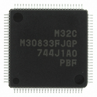
M30833FJGP#U3 Renesas Electronics America, M30833FJGP#U3 Datasheet - Page 314

M30833FJGP#U3
Manufacturer Part Number
M30833FJGP#U3
Description
IC M32C/83 MCU FLASH 100LQFP
Manufacturer
Renesas Electronics America
Series
M16C™ M32C/80r
Datasheets
1.M3087BFLGPU3.pdf
(364 pages)
2.M30833FJGPU3.pdf
(96 pages)
3.M30833FJGPU3.pdf
(529 pages)
Specifications of M30833FJGP#U3
Core Processor
M32C/80
Core Size
16/32-Bit
Speed
32MHz
Connectivity
CAN, I²C, IEBus, SIO, UART/USART
Peripherals
DMA, WDT
Number Of I /o
85
Program Memory Size
512KB (512K x 8)
Program Memory Type
FLASH
Ram Size
31K x 8
Voltage - Supply (vcc/vdd)
3 V ~ 5.5 V
Data Converters
A/D 26x10b; D/A 2x8b
Oscillator Type
Internal
Operating Temperature
-40°C ~ 85°C
Package / Case
100-LQFP
Package
100LQFP
Family Name
R8C
Maximum Speed
32 MHz
Operating Supply Voltage
5 V
Data Bus Width
16 Bit
Number Of Programmable I/os
87
Interface Type
UART
On-chip Adc
26-chx10-bit
On-chip Dac
2-chx8-bit
Number Of Timers
11
For Use With
R0K330879S001BE - KIT DEV RSK M32C/87R0K330879S000BE - KIT DEV RSK M32C/87
Lead Free Status / RoHS Status
Lead free / RoHS Compliant
Eeprom Size
-
Available stocks
Company
Part Number
Manufacturer
Quantity
Price
- Current page: 314 of 529
- Download datasheet (5Mb)
R
R
M
21.4 Communication Unit 0 and 1 Communication Function
e
E
3
. v
J
2
Figure 21.32 G0RI to G1RI Registers and G0TO to G1TO Registers
0
The communication function is available when two 8-bit shift registers are used with either timer measure-
ment function or waveform generation function.
In the intelligent I/O groups 0 and 1, 8-bit clock synchronous serial I/O, 8-bit clock asynchronous serial I/O
(UART) and HDLC data processing are available.
Figures 21.32 to 21.38 show registers associated with the communication function.
1
C
9
3 .
B
8 /
0
1
3
0
3
J
G
Group i Receive Input Register (i=0,1)
b7
4
Group i Transmit Output Register (i=0,1)
b7
a
0 -
n
o r
3 .
1
u
, 1
3
p
1
2
(
M
0
0
3
6
2
C
8 /
Page 289
, 3
M
3
b0
b0
2
C
f o
8 /
Set data to be transmitted to a received
data generation circuit
Can read data transmitted by a transmitted data generation circuit
4
3
8
Symbol
G0RI,G1RI
) T
Symbol
G0TO, G1TO
8
Function
21. Intelligent I/O (Group 0, 1 Communication Function)
Function
Address
00EC
Address
00EE
16
16
, 012C
, 012E
16
16
Setting Range
00
16
to FF
After Reset
Indeterminate
After Reset
Indeterminate
16
RW
WO
RW
RO
Related parts for M30833FJGP#U3
Image
Part Number
Description
Manufacturer
Datasheet
Request
R

Part Number:
Description:
KIT STARTER FOR M16C/29
Manufacturer:
Renesas Electronics America
Datasheet:

Part Number:
Description:
KIT STARTER FOR R8C/2D
Manufacturer:
Renesas Electronics America
Datasheet:

Part Number:
Description:
R0K33062P STARTER KIT
Manufacturer:
Renesas Electronics America
Datasheet:

Part Number:
Description:
KIT STARTER FOR R8C/23 E8A
Manufacturer:
Renesas Electronics America
Datasheet:

Part Number:
Description:
KIT STARTER FOR R8C/25
Manufacturer:
Renesas Electronics America
Datasheet:

Part Number:
Description:
KIT STARTER H8S2456 SHARPE DSPLY
Manufacturer:
Renesas Electronics America
Datasheet:

Part Number:
Description:
KIT STARTER FOR R8C38C
Manufacturer:
Renesas Electronics America
Datasheet:

Part Number:
Description:
KIT STARTER FOR R8C35C
Manufacturer:
Renesas Electronics America
Datasheet:

Part Number:
Description:
KIT STARTER FOR R8CL3AC+LCD APPS
Manufacturer:
Renesas Electronics America
Datasheet:

Part Number:
Description:
KIT STARTER FOR RX610
Manufacturer:
Renesas Electronics America
Datasheet:

Part Number:
Description:
KIT STARTER FOR R32C/118
Manufacturer:
Renesas Electronics America
Datasheet:

Part Number:
Description:
KIT DEV RSK-R8C/26-29
Manufacturer:
Renesas Electronics America
Datasheet:

Part Number:
Description:
KIT STARTER FOR SH7124
Manufacturer:
Renesas Electronics America
Datasheet:

Part Number:
Description:
KIT STARTER FOR H8SX/1622
Manufacturer:
Renesas Electronics America
Datasheet:

Part Number:
Description:
KIT DEV FOR SH7203
Manufacturer:
Renesas Electronics America
Datasheet:


