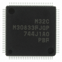
M30833FJGP#U3 Renesas Electronics America, M30833FJGP#U3 Datasheet - Page 521

M30833FJGP#U3
Manufacturer Part Number
M30833FJGP#U3
Description
IC M32C/83 MCU FLASH 100LQFP
Manufacturer
Renesas Electronics America
Series
M16C™ M32C/80r
Datasheets
1.M3087BFLGPU3.pdf
(364 pages)
2.M30833FJGPU3.pdf
(96 pages)
3.M30833FJGPU3.pdf
(529 pages)
Specifications of M30833FJGP#U3
Core Processor
M32C/80
Core Size
16/32-Bit
Speed
32MHz
Connectivity
CAN, I²C, IEBus, SIO, UART/USART
Peripherals
DMA, WDT
Number Of I /o
85
Program Memory Size
512KB (512K x 8)
Program Memory Type
FLASH
Ram Size
31K x 8
Voltage - Supply (vcc/vdd)
3 V ~ 5.5 V
Data Converters
A/D 26x10b; D/A 2x8b
Oscillator Type
Internal
Operating Temperature
-40°C ~ 85°C
Package / Case
100-LQFP
Package
100LQFP
Family Name
R8C
Maximum Speed
32 MHz
Operating Supply Voltage
5 V
Data Bus Width
16 Bit
Number Of Programmable I/os
87
Interface Type
UART
On-chip Adc
26-chx10-bit
On-chip Dac
2-chx8-bit
Number Of Timers
11
For Use With
R0K330879S001BE - KIT DEV RSK M32C/87R0K330879S000BE - KIT DEV RSK M32C/87
Lead Free Status / RoHS Status
Lead free / RoHS Compliant
Eeprom Size
-
Available stocks
Company
Part Number
Manufacturer
Quantity
Price
- Current page: 521 of 529
- Download datasheet (5Mb)
Rev.
REVISION HISTORY
Date
238 to 247 Sequence of the following Chapters have been changed: D/A Converter, CRC
226, 227 • Figure 17.2 AD0CON0 Register, Figure 17.3 AD0CON1 Register
229, 230 • Figure 17.5 AD1CON0 Register, Figure 17.6 AD1CON1 Register
Page
221
223
232
235
237
248
251
252
263
266
265
266
267
270
271
272
273
274
275
• Figure 16.32 SIM Interface Format modified
A/D Converter
Sequence of content modified
• Table 17.1 A/D Converter Specifications Explanaition of A/D Conversion
• Table 17.4 One-shot Mode Specifications Explanation of Start Condition
• Table 17.9 Trigger Select Function Settings Table modified; Note 2 added
• Figure 17.9 Analog Input Pin and External Sensor Equivalent Circuit
Intelligent I/O
• Figure 21.2 Intelligent I/O Group 1 Block Diagram modified
• Figure 21.5 G0BT to G3BT Registers and G0BCR0 to G3BCR0 Registers
• Table 21.2 Base Timer Specifications Explanation of Counter increment/
• Tables 21.3, 21.6, 21.8, 21.17, 21.23, 21.29, 21.31, 21.37, and 21,42
• Figure 21.18 Counter Increment Mode (Group 0 and 1) modified
• Figure 21.19 Counter Increment/Decrement Mode (Group 0 and 1) modified
• Figure 21.20 Base Timer Operation in Two-Phase Pulse Signal Processing
• 21.2 Time Measurement Function (Group 0 and 1) Contents added
• Figure 21.22 Time Measurement Function (2) modified
• Figure 21.23 Prescaler Function and Gate Function Diagram modified; Note
• Table 21.7 Pin Settings for Waveform Generation Function modified
• Table 21.8 Waveform Generation Function Associated Register Settings
• 21.3.1 Single-Phase Waveform Output Mode (Group 0 to 3) revised
• Table 21.9 Single-Phase Waveform Output Mode Specifications revised
• Figure 21.24 Single-Phase Waveform Output Mode modified
Start Conditions revised;
frequency modified
frequency modified
revised
Capacitance of the capacitor modified
Calculation, XY Conversion
Note 2 added to G0BT to G3BT registers, Note 3 deleted from G0BCR0 to
G3BCR0 registers
decrement mode in Selectable Function modified
Associated Register Settings Point of reference deleted
Mode Note 1 revised
2 of Gate Function deleted
Note 1 added
M32C/83 GROUP (M32C/83, M32C/83T) Hardware Manual
C-8
A/D frequency modified
Description
Summary
A/D
A/D
Related parts for M30833FJGP#U3
Image
Part Number
Description
Manufacturer
Datasheet
Request
R

Part Number:
Description:
KIT STARTER FOR M16C/29
Manufacturer:
Renesas Electronics America
Datasheet:

Part Number:
Description:
KIT STARTER FOR R8C/2D
Manufacturer:
Renesas Electronics America
Datasheet:

Part Number:
Description:
R0K33062P STARTER KIT
Manufacturer:
Renesas Electronics America
Datasheet:

Part Number:
Description:
KIT STARTER FOR R8C/23 E8A
Manufacturer:
Renesas Electronics America
Datasheet:

Part Number:
Description:
KIT STARTER FOR R8C/25
Manufacturer:
Renesas Electronics America
Datasheet:

Part Number:
Description:
KIT STARTER H8S2456 SHARPE DSPLY
Manufacturer:
Renesas Electronics America
Datasheet:

Part Number:
Description:
KIT STARTER FOR R8C38C
Manufacturer:
Renesas Electronics America
Datasheet:

Part Number:
Description:
KIT STARTER FOR R8C35C
Manufacturer:
Renesas Electronics America
Datasheet:

Part Number:
Description:
KIT STARTER FOR R8CL3AC+LCD APPS
Manufacturer:
Renesas Electronics America
Datasheet:

Part Number:
Description:
KIT STARTER FOR RX610
Manufacturer:
Renesas Electronics America
Datasheet:

Part Number:
Description:
KIT STARTER FOR R32C/118
Manufacturer:
Renesas Electronics America
Datasheet:

Part Number:
Description:
KIT DEV RSK-R8C/26-29
Manufacturer:
Renesas Electronics America
Datasheet:

Part Number:
Description:
KIT STARTER FOR SH7124
Manufacturer:
Renesas Electronics America
Datasheet:

Part Number:
Description:
KIT STARTER FOR H8SX/1622
Manufacturer:
Renesas Electronics America
Datasheet:

Part Number:
Description:
KIT DEV FOR SH7203
Manufacturer:
Renesas Electronics America
Datasheet:


