M30833FJGP#U3 Renesas Electronics America, M30833FJGP#U3 Datasheet - Page 89
M30833FJGP#U3
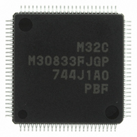
Manufacturer Part Number
M30833FJGP#U3
Description
IC M32C/83 MCU FLASH 100LQFP
Manufacturer
Renesas Electronics America
Series
M16C™ M32C/80r
Datasheets
1.M3087BFLGPU3.pdf
(364 pages)
2.M30833FJGPU3.pdf
(96 pages)
3.M30833FJGPU3.pdf
(529 pages)
Specifications of M30833FJGP#U3
Core Processor
M32C/80
Core Size
16/32-Bit
Speed
32MHz
Connectivity
CAN, I²C, IEBus, SIO, UART/USART
Peripherals
DMA, WDT
Number Of I /o
85
Program Memory Size
512KB (512K x 8)
Program Memory Type
FLASH
Ram Size
31K x 8
Voltage - Supply (vcc/vdd)
3 V ~ 5.5 V
Data Converters
A/D 26x10b; D/A 2x8b
Oscillator Type
Internal
Operating Temperature
-40°C ~ 85°C
Package / Case
100-LQFP
Package
100LQFP
Family Name
R8C
Maximum Speed
32 MHz
Operating Supply Voltage
5 V
Data Bus Width
16 Bit
Number Of Programmable I/os
87
Interface Type
UART
On-chip Adc
26-chx10-bit
On-chip Dac
2-chx8-bit
Number Of Timers
11
For Use With
R0K330879S001BE - KIT DEV RSK M32C/87R0K330879S000BE - KIT DEV RSK M32C/87
Lead Free Status / RoHS Status
Lead free / RoHS Compliant
Eeprom Size
-
Available stocks
Company
Part Number
Manufacturer
Quantity
Price


R
R
M
e
E
3
. v
J
Table 7.7 Microcomputer Status in a Hold State
Table 7.8 External Bus State when Accessing Internal Space
Table 7.9 RAS, CASL, CASH and DW Signals
2
________
0
Oscillation
RD Signal, WR Signal, Address Bus, Data Bus, BHE,
_______
CS0 to CS3
Programmable I/O Ports: P0 to P15
__________
HLDA
Internal Peripheral Circuits
ALE Signal
Address bus
Data Bus
RD, WR, WRL, WRH
BHE
_______
CS0 to CS3
ALE
_____
_____
Data Bus Width
7.2.8 External Bus State when Accessing Internal Space
7.2.9 BCLK Output
7.2.10 DRAM Control Signals (RAS, CASL, CASH and DW)
C
1
9
3 .
B
8 /
Table 7.8 shows external bus states when an internal space is accessed.
The CPU clock operates the CPU. When combining the PM07 bit in the PM0 register set to "0" (BCLK
output) and the CM01 to CM00 bits in the CM0 register set to "00
P5
No BCLK is output in single-chip mode. Refer to 8. Clock Generating Circuit for details.
The DRAM control signals control the DRAM. The DRAM control signals are output when the DRAM
area, determined by the AR0 to AR2 bits in the DRAMCONT register, is output. Table 7.9 lists each
signal operation.
0
1
3
16 bits
______
0
8 bits
3
3
J
G
4
as BCLK.
a
_______
_______
o r
0 -
n
3 .
________ _________
1
u
_______
, 1
3
p
Item
_____
1
(
2
M
When Read
When Write
0
0
3
__________
6
2
C
RAS
8 /
L
L
L
L
L
L
L
L
Page 64
, 3
__________
M
3
Item
2
C
f o
Holds an address of an external space accessed just before
High-impedance
High-impedance
Output "H"
Holds state of external space last accessed
Output "H"
Output ALE
CASL
8 /
H
4
L
L
H
L
L
L
L
3
8
) T
8
_____
State when accessing SFR, internal ROM and internal RAM
Not used
Not used
_______
CASH
H
H
L
L
L
L
__________
_______
DW
H
H
H
H
L
L
L
L
__________
On
High-impedance
Maintains the same state as when HOLD signal
is received
Output "L"
On (excluding the watchdog timer)
Output "L"
Read 1-byte data
Write 1-byte data
Read data from both even and odd addresses
Read 1-byte data from even address
Read 1-byte data from odd address
Write data to both even and odd addresses
Write 1-byte data to even address
Write 1-byte data to odd address
2
", the CPU clock signal is output from
_____
Data Bus State
Status
__________
7. Bus
Related parts for M30833FJGP#U3
Image
Part Number
Description
Manufacturer
Datasheet
Request
R

Part Number:
Description:
KIT STARTER FOR M16C/29
Manufacturer:
Renesas Electronics America
Datasheet:

Part Number:
Description:
KIT STARTER FOR R8C/2D
Manufacturer:
Renesas Electronics America
Datasheet:

Part Number:
Description:
R0K33062P STARTER KIT
Manufacturer:
Renesas Electronics America
Datasheet:

Part Number:
Description:
KIT STARTER FOR R8C/23 E8A
Manufacturer:
Renesas Electronics America
Datasheet:

Part Number:
Description:
KIT STARTER FOR R8C/25
Manufacturer:
Renesas Electronics America
Datasheet:

Part Number:
Description:
KIT STARTER H8S2456 SHARPE DSPLY
Manufacturer:
Renesas Electronics America
Datasheet:

Part Number:
Description:
KIT STARTER FOR R8C38C
Manufacturer:
Renesas Electronics America
Datasheet:

Part Number:
Description:
KIT STARTER FOR R8C35C
Manufacturer:
Renesas Electronics America
Datasheet:

Part Number:
Description:
KIT STARTER FOR R8CL3AC+LCD APPS
Manufacturer:
Renesas Electronics America
Datasheet:
Part Number:
Description:
KIT STARTER FOR RX610
Manufacturer:
Renesas Electronics America
Datasheet:

Part Number:
Description:
KIT STARTER FOR R32C/118
Manufacturer:
Renesas Electronics America
Datasheet:

Part Number:
Description:
KIT DEV RSK-R8C/26-29
Manufacturer:
Renesas Electronics America
Datasheet:

Part Number:
Description:
KIT STARTER FOR SH7124
Manufacturer:
Renesas Electronics America
Datasheet:

Part Number:
Description:
KIT STARTER FOR H8SX/1622
Manufacturer:
Renesas Electronics America
Datasheet:

Part Number:
Description:
KIT DEV FOR SH7203
Manufacturer:
Renesas Electronics America
Datasheet: