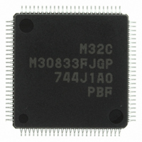
M30833FJGP#U3 Renesas Electronics America, M30833FJGP#U3 Datasheet - Page 295

M30833FJGP#U3
Manufacturer Part Number
M30833FJGP#U3
Description
IC M32C/83 MCU FLASH 100LQFP
Manufacturer
Renesas Electronics America
Series
M16C™ M32C/80r
Datasheets
1.M3087BFLGPU3.pdf
(364 pages)
2.M30833FJGPU3.pdf
(96 pages)
3.M30833FJGPU3.pdf
(529 pages)
Specifications of M30833FJGP#U3
Core Processor
M32C/80
Core Size
16/32-Bit
Speed
32MHz
Connectivity
CAN, I²C, IEBus, SIO, UART/USART
Peripherals
DMA, WDT
Number Of I /o
85
Program Memory Size
512KB (512K x 8)
Program Memory Type
FLASH
Ram Size
31K x 8
Voltage - Supply (vcc/vdd)
3 V ~ 5.5 V
Data Converters
A/D 26x10b; D/A 2x8b
Oscillator Type
Internal
Operating Temperature
-40°C ~ 85°C
Package / Case
100-LQFP
Package
100LQFP
Family Name
R8C
Maximum Speed
32 MHz
Operating Supply Voltage
5 V
Data Bus Width
16 Bit
Number Of Programmable I/os
87
Interface Type
UART
On-chip Adc
26-chx10-bit
On-chip Dac
2-chx8-bit
Number Of Timers
11
For Use With
R0K330879S001BE - KIT DEV RSK M32C/87R0K330879S000BE - KIT DEV RSK M32C/87
Lead Free Status / RoHS Status
Lead free / RoHS Compliant
Eeprom Size
-
Available stocks
Company
Part Number
Manufacturer
Quantity
Price
- Current page: 295 of 529
- Download datasheet (5Mb)
R
R
M
e
E
3
. v
J
2
0
Table 21.5 Pin Settings for Time Measurement Function
NOTES:
Table 21.6 Time Measurement Function Associated Register Settings
i = 0 to 1;
Bit configurations and functions vary with channels and groups used.
Registers associated with the time measurement function must be set after setting registers associated with the base timer.
P7
P7
P7
P7
P8
P11
P11
P14
P14
P15
P15
P15
P15
P15
P15
P15
P15
GiTMCRj
GiTPRk
GiFS
GiFE
C
1
9
3 .
B
8 /
1. This port is provided in the 144-pin package only.
2. Apply trigger to INPC0j pin (j=0 to 7) when the CAS bit in the GiBCR register is set to "1" (32-bit time measurement
4
5
6
7
0
Register
0
1
/INPC1
/INPC1
/INPC0
/INPC0
/INPC0
3
1
2
2
3
0
1
2
3
4
5
6
7
0
function). Trigger input to INPC1k pin (k=1, 2, 6, 7) is invalid.
/INPC1
/INPC1
/INPC1
/INPC1
/INPC0
/INPC0
/INPC0
/INPC0
/INPC0
/INPC0
/INPC0
/INPC0
3
J
G
4
a
o r
0 -
n
Pin
3 .
1
u
j = 0 to 7;
1
2
0
1
2
, 1
3
p
(2)
1 (1)
2 (1)
6 (1)
7 (1)
0 (1)
1 (1)
2 (1)
3 (1)
4 (1)
5 (1)
6 (1)
7 (1)
1
(
2
M
0
0
3
CTS1 to CTS0
DF1 to DF0
GT, GOC, GSC
PR
-
FSCj
IFEj
6
2
C
8 /
Page 270
k = 6, 7
, 3
PS1, PS2, PS5, PS8, PS9
Registers
PS1_4 = 0
PS1_5 = 0
PS1_6 = 0
PS1_7 = 0
PS2_0 = 0
PS5_1 = 0
PS5_2 = 0
PS8_2 = 0
PS8_3 = 0
PS9_0 = 0
PS9_1 = 0
PS9_4 = 0
PS9_5 = 0
Bit
M
3
2
C
f o
8 /
4
3
8
) T
8
Select a time measurement trigger
Select the digital filter function
Select the gate function
Select the prescaler function
Setting value of the prescaler
Set to "1" (time measurement function)
Set to "1" (channel j function enabled)
PD7, PD8, PD11, PD14, PD15
Registers
PD7_4 = 0
PD7_5 = 0
PD7_6 = 0
PD7_7 = 0
PD8_0 = 0
PD11_1 = 0
PD11_2 = 0
PD14_2 = 0
PD14_3 = 0
PD15_0 = 0
PD15_1 = 0
PD15_2 = 0
PD15_3 = 0
PD15_4 = 0
PD15_5 = 0
PD15_6 = 0
PD15_7 = 0
Bit and Setting
21. Intelligent I/O (Time Measurement Function)
Function
IPS Register
IPS1 = 0
IPS0 = 0
IPS1 =1
IPS0 = 1, IPS2 = 0
IPS2 = 0
Related parts for M30833FJGP#U3
Image
Part Number
Description
Manufacturer
Datasheet
Request
R

Part Number:
Description:
KIT STARTER FOR M16C/29
Manufacturer:
Renesas Electronics America
Datasheet:

Part Number:
Description:
KIT STARTER FOR R8C/2D
Manufacturer:
Renesas Electronics America
Datasheet:

Part Number:
Description:
R0K33062P STARTER KIT
Manufacturer:
Renesas Electronics America
Datasheet:

Part Number:
Description:
KIT STARTER FOR R8C/23 E8A
Manufacturer:
Renesas Electronics America
Datasheet:

Part Number:
Description:
KIT STARTER FOR R8C/25
Manufacturer:
Renesas Electronics America
Datasheet:

Part Number:
Description:
KIT STARTER H8S2456 SHARPE DSPLY
Manufacturer:
Renesas Electronics America
Datasheet:

Part Number:
Description:
KIT STARTER FOR R8C38C
Manufacturer:
Renesas Electronics America
Datasheet:

Part Number:
Description:
KIT STARTER FOR R8C35C
Manufacturer:
Renesas Electronics America
Datasheet:

Part Number:
Description:
KIT STARTER FOR R8CL3AC+LCD APPS
Manufacturer:
Renesas Electronics America
Datasheet:

Part Number:
Description:
KIT STARTER FOR RX610
Manufacturer:
Renesas Electronics America
Datasheet:

Part Number:
Description:
KIT STARTER FOR R32C/118
Manufacturer:
Renesas Electronics America
Datasheet:

Part Number:
Description:
KIT DEV RSK-R8C/26-29
Manufacturer:
Renesas Electronics America
Datasheet:

Part Number:
Description:
KIT STARTER FOR SH7124
Manufacturer:
Renesas Electronics America
Datasheet:

Part Number:
Description:
KIT STARTER FOR H8SX/1622
Manufacturer:
Renesas Electronics America
Datasheet:

Part Number:
Description:
KIT DEV FOR SH7203
Manufacturer:
Renesas Electronics America
Datasheet:


