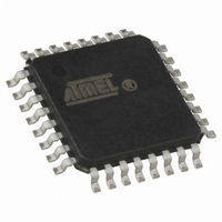
ATMEGA16M1-AU Atmel, ATMEGA16M1-AU Datasheet - Page 100

ATMEGA16M1-AU
Manufacturer Part Number
ATMEGA16M1-AU
Description
IC MCU AVR 16K FLASH 32TQFP
Manufacturer
Atmel
Series
AVR® ATmegar
Specifications of ATMEGA16M1-AU
Core Processor
AVR
Core Size
8-Bit
Speed
16MHz
Connectivity
CAN, LIN, SPI, UART/USART
Peripherals
Brown-out Detect/Reset, POR, PWM, Temp Sensor, WDT
Program Memory Size
16KB (8K x 16)
Program Memory Type
FLASH
Eeprom Size
512 x 8
Ram Size
1K x 8
Voltage - Supply (vcc/vdd)
2.7 V ~ 5.5 V
Data Converters
A/D 11x10b; D/A 1x10b
Oscillator Type
Internal
Operating Temperature
-40°C ~ 85°C
Package / Case
32-TQFP, 32-VQFP
Lead Free Status / RoHS Status
Lead free / RoHS Compliant
Number Of I /o
-
Available stocks
Company
Part Number
Manufacturer
Quantity
Price
- Current page: 100 of 341
- Download datasheet (6Mb)
14.9.3
14.9.4
14.9.5
14.9.6
100
ATmega16M1/32M1/64M1
TCNT0 – Timer/Counter Register
OCR0A – Output Compare Register A
OCR0B – Output Compare Register B
TIMSK0 – Timer/Counter Interrupt Mask Register
Table 14-9.
If external pin modes are used for the Timer/Counter0, transitions on the T0 pin will clock the
counter even if the pin is configured as an output. This feature allows software control of the
counting.
The Timer/Counter Register gives direct access, both for read and write operations, to the
Timer/Counter unit 8-bit counter. Writing to the TCNT0 Register blocks (removes) the Compare
Match on the following timer clock. Modifying the counter (TCNT0) while the counter is running,
introduces a risk of missing a Compare Match between TCNT0 and the OCR0x Registers.
The Output Compare Register A contains an 8-bit value that is continuously compared with the
counter value (TCNT0). A match can be used to generate an Output Compare interrupt, or to
generate a waveform output on the OC0A pin.
The Output Compare Register B contains an 8-bit value that is continuously compared with the
counter value (TCNT0). A match can be used to generate an Output Compare interrupt, or to
generate a waveform output on the OC0B pin.
• Bits 7:3 – Res: Reserved
These bits are reserved and will always read as zero.
Bit
Read/Write
Initial Value
Bit
Read/Write
Initial Value
Bit
Read/Write
Initial Value
Bit
Read/Write
Initial Value
CS02
1
1
1
1
CS01
0
0
1
1
Clock Select Bit Description (Continued)
R/W
R/W
R/W
R
7
–
0
7
0
7
0
7
0
CS00
0
1
0
1
R/W
R/W
R/W
R
6
–
0
6
0
6
0
6
0
Description
clk
clk
External clock source on T0 pin. Clock on falling edge
External clock source on T0 pin. Clock on rising edge
I/O
I/O
/256 (From prescaler)
/1024 (From prescaler)
R/W
R/W
R/W
5
–
R
0
5
0
5
0
5
0
R/W
R/W
R/W
R
4
–
0
4
0
4
0
4
0
OCR0A[7:0]
OCR0B[7:0]
TCNT0[7:0]
R/W
R/W
R/W
R
3
–
0
3
0
3
0
3
0
OCIE0B
R/W
R/W
R/W
R/W
2
0
2
0
2
0
2
0
OCIE0A
R/W
R/W
R/W
R/W
1
0
1
0
1
0
1
0
TOIE0
R/W
R/W
R/W
R/W
0
0
0
0
0
0
0
0
8209D–AVR–11/10
OCR0A
OCR0B
TIMSK0
TCNT0
Related parts for ATMEGA16M1-AU
Image
Part Number
Description
Manufacturer
Datasheet
Request
R

Part Number:
Description:
Manufacturer:
Atmel Corporation
Datasheet:

Part Number:
Description:
IC AVR MCU 16K 16MHZ 5V 44TQFP
Manufacturer:
Atmel
Datasheet:

Part Number:
Description:
IC AVR MCU 16K 16MHZ 5V 44-QFN
Manufacturer:
Atmel
Datasheet:

Part Number:
Description:
IC AVR MCU 16K 16MHZ 5V 40DIP
Manufacturer:
Atmel
Datasheet:

Part Number:
Description:
MCU AVR 16K FLASH 16MHZ 44-QFN
Manufacturer:
Atmel
Datasheet:

Part Number:
Description:
IC AVR MCU 16K 16MHZ COM 40-DIP
Manufacturer:
Atmel
Datasheet:

Part Number:
Description:
IC AVR MCU 16K 16MHZ COM 44-QFN
Manufacturer:
Atmel
Datasheet:

Part Number:
Description:
IC AVR MCU 16K 16MHZ IND 40-DIP
Manufacturer:
Atmel
Datasheet:

Part Number:
Description:
IC AVR MCU 16K 16MHZ IND 44-QFN
Manufacturer:
Atmel
Datasheet:

Part Number:
Description:
IC AVR MCU 16K 16MHZ IND 44-TQFP
Manufacturer:
Atmel
Datasheet:

Part Number:
Description:
IC MCU 8BIT 16KB FLASH 44TQFP
Manufacturer:
Atmel
Datasheet:

Part Number:
Description:
MCU AVR 16K FLASH 16MHZ 44-TQFP
Manufacturer:
Atmel
Datasheet:

Part Number:
Description:
IC AVR MCU 16K 16MHZ COM 44-TQFP
Manufacturer:
Atmel
Datasheet:


