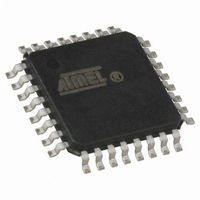
ATMEGA16M1-AU Atmel, ATMEGA16M1-AU Datasheet - Page 234

ATMEGA16M1-AU
Manufacturer Part Number
ATMEGA16M1-AU
Description
IC MCU AVR 16K FLASH 32TQFP
Manufacturer
Atmel
Series
AVR® ATmegar
Specifications of ATMEGA16M1-AU
Core Processor
AVR
Core Size
8-Bit
Speed
16MHz
Connectivity
CAN, LIN, SPI, UART/USART
Peripherals
Brown-out Detect/Reset, POR, PWM, Temp Sensor, WDT
Program Memory Size
16KB (8K x 16)
Program Memory Type
FLASH
Eeprom Size
512 x 8
Ram Size
1K x 8
Voltage - Supply (vcc/vdd)
2.7 V ~ 5.5 V
Data Converters
A/D 11x10b; D/A 1x10b
Oscillator Type
Internal
Operating Temperature
-40°C ~ 85°C
Package / Case
32-TQFP, 32-VQFP
Lead Free Status / RoHS Status
Lead free / RoHS Compliant
Number Of I /o
-
Available stocks
Company
Part Number
Manufacturer
Quantity
Price
- Current page: 234 of 341
- Download datasheet (6Mb)
21.7
234
ADC Conversion Result
ATmega16M1/32M1/64M1
Figure 21-13. Differential Non-linearity (DNL)
After the conversion is complete (ADIF is high), the conversion result can be found in the ADC
Result Registers (ADCL, ADCH).
For single ended conversion, the result is:
where V
Table 21-4 on page 242
0x3FF represents the selected reference voltage.
If differential channels are used, the result is:
where V
GAIN the selected gain factor and V
in two’s complement form, from 0x200 (-512d) through 0x1FF (+511d). Note that if the user
wants to perform a quick polarity check of the result, it is sufficient to read the MSB of the result
(ADC9 in ADCH). If the bit is one, the result is negative, and if this bit is zero, the result is posi-
tive.
Table 21-2 on page 235
(ADCn - ADCm) is selected with a reference voltage of V
• Quantization Error: Due to the quantization of the input voltage into a finite number of codes,
• Absolute Accuracy: The maximum deviation of an actual (unadjusted) transition compared to
a range of input voltages (1 LSB wide) will code to the same value. Always ±0.5 LSB
an ideal transition for any code. This is the compound effect of offset, gain error, differential
error, non-linearity, and quantization error. Ideal value: ±0.5 LSB
Figure 21-14 on page 235
IN
POS
is the voltage on the selected input pin and V
is the voltage on the positive input pin, V
Output Code
0x000
0x3FF
and
shows the resulting output codes if the differential input channel pair
0
Table 21-5 on page
shows the decoding of the differential input range.
1 LSB
ADC
REF
ADC
=
the selected voltage reference. The result is presented
(
----------------------------------------------------------------------- -
V
POS
=
V
--------------------------
–
IN
V
243). 0x000 represents analog ground, and
V
⋅
REF
NEG
1023
NEG
V
REF
REF
) GAIN 512
REF
⋅
the voltage on the negative input pin,
.
the selected voltage reference (see
V
⋅
REF
Input Voltage
8209D–AVR–11/10
Related parts for ATMEGA16M1-AU
Image
Part Number
Description
Manufacturer
Datasheet
Request
R

Part Number:
Description:
Manufacturer:
Atmel Corporation
Datasheet:

Part Number:
Description:
IC AVR MCU 16K 16MHZ 5V 44TQFP
Manufacturer:
Atmel
Datasheet:

Part Number:
Description:
IC AVR MCU 16K 16MHZ 5V 44-QFN
Manufacturer:
Atmel
Datasheet:

Part Number:
Description:
IC AVR MCU 16K 16MHZ 5V 40DIP
Manufacturer:
Atmel
Datasheet:

Part Number:
Description:
MCU AVR 16K FLASH 16MHZ 44-QFN
Manufacturer:
Atmel
Datasheet:

Part Number:
Description:
IC AVR MCU 16K 16MHZ COM 40-DIP
Manufacturer:
Atmel
Datasheet:

Part Number:
Description:
IC AVR MCU 16K 16MHZ COM 44-QFN
Manufacturer:
Atmel
Datasheet:

Part Number:
Description:
IC AVR MCU 16K 16MHZ IND 40-DIP
Manufacturer:
Atmel
Datasheet:

Part Number:
Description:
IC AVR MCU 16K 16MHZ IND 44-QFN
Manufacturer:
Atmel
Datasheet:

Part Number:
Description:
IC AVR MCU 16K 16MHZ IND 44-TQFP
Manufacturer:
Atmel
Datasheet:

Part Number:
Description:
IC MCU 8BIT 16KB FLASH 44TQFP
Manufacturer:
Atmel
Datasheet:

Part Number:
Description:
MCU AVR 16K FLASH 16MHZ 44-TQFP
Manufacturer:
Atmel
Datasheet:

Part Number:
Description:
IC AVR MCU 16K 16MHZ COM 44-TQFP
Manufacturer:
Atmel
Datasheet:


