ST7FLITE49K2T6TR STMicroelectronics, ST7FLITE49K2T6TR Datasheet - Page 142
ST7FLITE49K2T6TR
Manufacturer Part Number
ST7FLITE49K2T6TR
Description
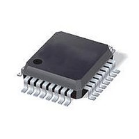
IC MCU 8BIT 8K FLASH 32LQFP
Manufacturer
STMicroelectronics
Series
ST7r
Datasheet
1.ST7FLITE49K2T6TR.pdf
(245 pages)
Specifications of ST7FLITE49K2T6TR
Core Processor
ST7
Core Size
8-Bit
Speed
8MHz
Connectivity
I²C, SPI
Peripherals
LVD, POR, PWM, WDT
Number Of I /o
24
Program Memory Size
8KB (8K x 8)
Program Memory Type
FLASH
Eeprom Size
256 x 8
Ram Size
384 x 8
Voltage - Supply (vcc/vdd)
2.4 V ~ 5.5 V
Data Converters
A/D 10x10b
Oscillator Type
Internal
Operating Temperature
-40°C ~ 85°C
Package / Case
32-LQFP
Processor Series
ST7FLITE4x
Core
ST7
Data Bus Width
8 bit
Data Ram Size
384 B
Interface Type
I2C, SPI
Maximum Clock Frequency
8 MHz
Number Of Programmable I/os
24
Number Of Timers
4
Maximum Operating Temperature
+ 85 C
Mounting Style
SMD/SMT
Development Tools By Supplier
ST7FLITE-SK/RAIS, ST7FLI49M-D/RAIS, STX-RLINK
Minimum Operating Temperature
- 40 C
On-chip Adc
10 bit, 10 Channel
For Use With
497-8399 - BOARD EVAL ST7LITE49M/STLED316S497-5858 - EVAL BOARD PLAYBACK ST7FLITE
Lead Free Status / RoHS Status
Lead free / RoHS Compliant
Available stocks
Company
Part Number
Manufacturer
Quantity
Price
Company:

Part Number:
ST7FLITE49K2T6TR
Manufacturer:
STMicroelectronics
Quantity:
10 000


On-chip peripherals
11.5.4
Slave mode
Note:
142/245
Functional description
Refer to the CR, SR1 and SR2 registers in
By default the I
initiates a transmit or receive sequence.
First the interface frequency must be configured using the FRi bits in the OAR2 register.
As soon as a start condition is detected, the address is received from the SDA line and sent
to the shift register; then it is compared with the address of the interface or the General Call
address (if selected by software).
In 10-bit addressing mode, the comparison includes the header sequence (11110xx0) and
the two most significant bits of the address.
●
●
●
Then the interface waits for a read of the SR1 register, holding the SCL line low (see
Figure 71
Next, in 7-bit mode read the DR register to determine from the least significant bit (Data
Direction Bit) if the slave must enter Receiver or Transmitter mode.
In 10-bit mode, after receiving the address sequence the slave is always in receive mode. It
will enter transmit mode on receiving a repeated Start condition followed by the header
sequence with matching address bits and the least significant bit set (11110xx1).
Slave receiver
Following the address reception and after SR1 register has been read, the slave receives
bytes from the SDA line into the DR register via the internal shift register. After each byte
the interface generates in sequence:
●
●
Then the interface waits for a read of the SR1 register followed by a read of the DR register,
holding the SCL line low (see
Slave transmitter
Following the address reception and after SR1 register has been read, the slave sends
bytes from the DR register to the SDA line via the internal shift register.
The slave waits for a read of the SR1 register followed by a write in the DR register, holding
the SCL line low (see
When the acknowledge pulse is received the EVF and BTF bits are set by hardware with an
interrupt if the ITE bit is set.
Header matched (10-bit mode only): the interface generates an acknowledge pulse if
the ACK bit is set.
Address not matched: the interface ignores it and waits for another Start condition.
Address matched: the interface generates in sequence:
–
–
Acknowledge pulse if the ACK bit is set
EVF and BTF bits are set with an interrupt if the ITE bit is set.
Acknowledge pulse if the ACK bit is set.
EVF and ADSL bits are set with an interrupt if the ITE bit is set.
Transfer sequencing EV1).
2
C interface operates in Slave mode (M/SL bit is cleared) except when it
Figure 71
Figure 71
Transfer sequencing EV3).
Transfer sequencing EV2).
Section
11.5.7. for the bit definitions.
ST7LITE49K2
Related parts for ST7FLITE49K2T6TR
Image
Part Number
Description
Manufacturer
Datasheet
Request
R

Part Number:
Description:
STMicroelectronics [RIPPLE-CARRY BINARY COUNTER/DIVIDERS]
Manufacturer:
STMicroelectronics
Datasheet:
Part Number:
Description:
STMicroelectronics [LIQUID-CRYSTAL DISPLAY DRIVERS]
Manufacturer:
STMicroelectronics
Datasheet:

Part Number:
Description:
BOARD EVAL FOR MEMS SENSORS
Manufacturer:
STMicroelectronics
Datasheet:
Part Number:
Description:
NPN TRANSISTOR POWER MODULE
Manufacturer:
STMicroelectronics
Datasheet:
Part Number:
Description:
TURBOSWITCH ULTRA-FAST HIGH VOLTAGE DIODE
Manufacturer:
STMicroelectronics
Datasheet:
Part Number:
Description:
Manufacturer:
STMicroelectronics
Datasheet:
Part Number:
Description:
DIODE / SCR MODULE
Manufacturer:
STMicroelectronics
Datasheet:
Part Number:
Description:
DIODE / SCR MODULE
Manufacturer:
STMicroelectronics
Datasheet:
Part Number:
Description:
Search -----> STE16N100
Manufacturer:
STMicroelectronics
Datasheet:
Part Number:
Description:
Search ---> STE53NA50
Manufacturer:
STMicroelectronics
Datasheet:
Part Number:
Description:
NPN Transistor Power Module
Manufacturer:
STMicroelectronics
Datasheet:
Part Number:
Description:
DIODE / SCR MODULE
Manufacturer:
STMicroelectronics
Datasheet: