ST7FLITE49K2T6 STMicroelectronics, ST7FLITE49K2T6 Datasheet - Page 20
ST7FLITE49K2T6
Manufacturer Part Number
ST7FLITE49K2T6
Description
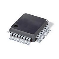
IC MCU 8BIT 8K FLASH 32LQFP
Manufacturer
STMicroelectronics
Series
ST7r
Datasheet
1.ST7FLITE49K2T6TR.pdf
(245 pages)
Specifications of ST7FLITE49K2T6
Core Processor
ST7
Core Size
8-Bit
Speed
8MHz
Connectivity
I²C, SPI
Peripherals
LVD, POR, PWM, WDT
Number Of I /o
24
Program Memory Size
8KB (8K x 8)
Program Memory Type
FLASH
Eeprom Size
256 x 8
Ram Size
384 x 8
Voltage - Supply (vcc/vdd)
2.4 V ~ 5.5 V
Data Converters
A/D 10x10b
Oscillator Type
Internal
Operating Temperature
-40°C ~ 85°C
Package / Case
32-LQFP
Processor Series
ST7FLITE4x
Core
ST7
Data Bus Width
8 bit
Data Ram Size
384 B
Interface Type
I2C, SPI
Maximum Clock Frequency
8 MHz
Number Of Programmable I/os
24
Number Of Timers
4
Maximum Operating Temperature
+ 85 C
Mounting Style
SMD/SMT
Development Tools By Supplier
ST7FLITE-SK/RAIS, ST7FLI49M-D/RAIS, STX-RLINK
Minimum Operating Temperature
- 40 C
On-chip Adc
10 bit, 10 Channel
For Use With
497-8399 - BOARD EVAL ST7LITE49M/STLED316S497-5858 - EVAL BOARD PLAYBACK ST7FLITE
Lead Free Status / RoHS Status
Lead free / RoHS Compliant
Available stocks
Company
Part Number
Manufacturer
Quantity
Price
Company:

Part Number:
ST7FLITE49K2T6
Manufacturer:
ST
Quantity:
3 000
Company:
Part Number:
ST7FLITE49K2T6
Manufacturer:
STMicroelectronics
Quantity:
10 000
Company:
Part Number:
ST7FLITE49K2T6TR
Manufacturer:
STMicroelectronics
Quantity:
10 000


Pin description
Table 2.
1. In the open-drain output column, T defines a true open-drain I/O (P-Buffer and protection diode to V
2. It is mandatory to connect all available V
20/245
26
27
28
29
30
31
32
number
implemented).0
Pin
30
31
32
1
2
3
4
PA2(HS)/ATPWM0 I/O
PC5/COMPINB+/
PC6/COMPINA+
PA0 /COMPINA-
ST7LITE49K2 device pin description
PC7/BREAK1/
PA1(HS)/ATIC
COMPOUTA
/OCMP1_A
COMPINB-
PC4/LTIC/
Pin name
BREAK2
I/O
I/O
I/O
I/O
I/O
I/O
DD
C
C
C
C
C
C
C
Level
T
T
T
T
T
T
T
and V
HS
HS
DDA
pins to the supply voltage and all V
x
x
x
x
x
x
x
Input
ei2
ei2
ei0
Port/control
Output
x
x
x
x
x
x
x
x
x
x
x
x
x
x
SS
and V
function
Port C4
Port C5
Port C6
Port C7
Port A0
Port A1
Port A2
reset)
(after
Main
(HS)
(HS)
SSA
DD
pins to ground.
are not
BREAK1/Ana
LTIC/Analog
Comparator
Comparator
Comparator
Comparator
comparator
Compare 1
Reference
Alternate
reference
ATPWM0
function
Output A
External
External
external
Timer A
Input B/
break 2
Input A/
Input B
Analog
Analog
Input A
Analog
Output
ST7LITE49K2
ATIC
log
Related parts for ST7FLITE49K2T6
Image
Part Number
Description
Manufacturer
Datasheet
Request
R

Part Number:
Description:
KIT STARTER RAISONANCE ST7FLITE
Manufacturer:
STMicroelectronics
Datasheet:

Part Number:
Description:
STMicroelectronics [RIPPLE-CARRY BINARY COUNTER/DIVIDERS]
Manufacturer:
STMicroelectronics
Datasheet:
Part Number:
Description:
STMicroelectronics [LIQUID-CRYSTAL DISPLAY DRIVERS]
Manufacturer:
STMicroelectronics
Datasheet:

Part Number:
Description:
BOARD EVAL FOR MEMS SENSORS
Manufacturer:
STMicroelectronics
Datasheet:
Part Number:
Description:
NPN TRANSISTOR POWER MODULE
Manufacturer:
STMicroelectronics
Datasheet:
Part Number:
Description:
TURBOSWITCH ULTRA-FAST HIGH VOLTAGE DIODE
Manufacturer:
STMicroelectronics
Datasheet:
Part Number:
Description:
Manufacturer:
STMicroelectronics
Datasheet:
Part Number:
Description:
DIODE / SCR MODULE
Manufacturer:
STMicroelectronics
Datasheet:
Part Number:
Description:
DIODE / SCR MODULE
Manufacturer:
STMicroelectronics
Datasheet:
Part Number:
Description:
Search -----> STE16N100
Manufacturer:
STMicroelectronics
Datasheet:
Part Number:
Description:
Search ---> STE53NA50
Manufacturer:
STMicroelectronics
Datasheet:
Part Number:
Description:
NPN Transistor Power Module
Manufacturer:
STMicroelectronics
Datasheet: