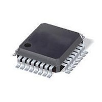
ST7FLITE49K2T6 STMicroelectronics, ST7FLITE49K2T6 Datasheet - Page 45

ST7FLITE49K2T6
Manufacturer Part Number
ST7FLITE49K2T6
Description
IC MCU 8BIT 8K FLASH 32LQFP
Manufacturer
STMicroelectronics
Series
ST7r
Datasheet
1.ST7FLITE49K2T6TR.pdf
(245 pages)
Specifications of ST7FLITE49K2T6
Core Processor
ST7
Core Size
8-Bit
Speed
8MHz
Connectivity
I²C, SPI
Peripherals
LVD, POR, PWM, WDT
Number Of I /o
24
Program Memory Size
8KB (8K x 8)
Program Memory Type
FLASH
Eeprom Size
256 x 8
Ram Size
384 x 8
Voltage - Supply (vcc/vdd)
2.4 V ~ 5.5 V
Data Converters
A/D 10x10b
Oscillator Type
Internal
Operating Temperature
-40°C ~ 85°C
Package / Case
32-LQFP
Processor Series
ST7FLITE4x
Core
ST7
Data Bus Width
8 bit
Data Ram Size
384 B
Interface Type
I2C, SPI
Maximum Clock Frequency
8 MHz
Number Of Programmable I/os
24
Number Of Timers
4
Maximum Operating Temperature
+ 85 C
Mounting Style
SMD/SMT
Development Tools By Supplier
ST7FLITE-SK/RAIS, ST7FLI49M-D/RAIS, STX-RLINK
Minimum Operating Temperature
- 40 C
On-chip Adc
10 bit, 10 Channel
For Use With
497-8399 - BOARD EVAL ST7LITE49M/STLED316S497-5858 - EVAL BOARD PLAYBACK ST7FLITE
Lead Free Status / RoHS Status
Lead free / RoHS Compliant
Available stocks
Company
Part Number
Manufacturer
Quantity
Price
Company:
Part Number:
ST7FLITE49K2T6
Manufacturer:
ST
Quantity:
3 000
Company:
Part Number:
ST7FLITE49K2T6
Manufacturer:
STMicroelectronics
Quantity:
10 000
Company:
Part Number:
ST7FLITE49K2T6TR
Manufacturer:
STMicroelectronics
Quantity:
10 000
ST7LITE49K2
7.3.2
7.3.3
7.3.4
Asynchronous external RESET pin
The RESET pin is both an input and an open-drain output with integrated R
resistor. This pull-up has no fixed value but varies in accordance with the input voltage. It
can be pulled low by external circuitry to reset the device. See Electrical Characteristic
section for more details.
A RESET signal originating from an external source must have a duration of at least
t
asynchronous and therefore the MCU can enter reset state even in Halt mode.
The RESET pin is an asynchronous signal which plays a major role in EMS performance. In
a noisy environment, it is recommended to follow the guidelines mentioned in the electrical
characteristics section.
Figure 15. Reset block diagram
1. See
External power-on reset
If the LVD is disabled by option byte, to start up the microcontroller correctly, the user must
ensure by means of an external reset circuit that the reset signal is held low until V
the minimum level specified for the selected f
A proper reset signal for a slow rising V
RC network connected to the RESET pin.
Internal low voltage detector (LVD) reset
Two different Reset sequences caused by the internal LVD circuitry can be distinguished:
●
●
The device RESET pin acts as an output that is pulled low when V
(rising edge) or V
The LVD filters spikes on V
h(RSTL)in
RESET
Power-on reset
Voltage drop reset
Section 12.2.1: Illegal opcode reset on page 189
in order to be recognized (see
DD
lower than V
V
DD
R
ON
DD
larger than t
IT-
Filter
(falling edge) as shown in
GENERATOR
DD
Figure 16: Reset
PULSE
g(VDD)
supply can generally be provided by an external
OSC
for more details on illegal opcode reset conditions.
to avoid parasitic resets.
frequency.
Supply, reset and clock management
sequences). This detection is
___
___
___
ILLEGAL OPCODE RESET
Figure 16.
LVD RESET
WATCHDOG RESET
DD
is lower than V
INTERNAL
RESET
ON
weak pull-up
DD
IT+
is over
1)
45/245


