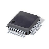
ST7FLITE49K2T6 STMicroelectronics, ST7FLITE49K2T6 Datasheet - Page 91

ST7FLITE49K2T6
Manufacturer Part Number
ST7FLITE49K2T6
Description
IC MCU 8BIT 8K FLASH 32LQFP
Manufacturer
STMicroelectronics
Series
ST7r
Datasheet
1.ST7FLITE49K2T6TR.pdf
(245 pages)
Specifications of ST7FLITE49K2T6
Core Processor
ST7
Core Size
8-Bit
Speed
8MHz
Connectivity
I²C, SPI
Peripherals
LVD, POR, PWM, WDT
Number Of I /o
24
Program Memory Size
8KB (8K x 8)
Program Memory Type
FLASH
Eeprom Size
256 x 8
Ram Size
384 x 8
Voltage - Supply (vcc/vdd)
2.4 V ~ 5.5 V
Data Converters
A/D 10x10b
Oscillator Type
Internal
Operating Temperature
-40°C ~ 85°C
Package / Case
32-LQFP
Processor Series
ST7FLITE4x
Core
ST7
Data Bus Width
8 bit
Data Ram Size
384 B
Interface Type
I2C, SPI
Maximum Clock Frequency
8 MHz
Number Of Programmable I/os
24
Number Of Timers
4
Maximum Operating Temperature
+ 85 C
Mounting Style
SMD/SMT
Development Tools By Supplier
ST7FLITE-SK/RAIS, ST7FLI49M-D/RAIS, STX-RLINK
Minimum Operating Temperature
- 40 C
On-chip Adc
10 bit, 10 Channel
For Use With
497-8399 - BOARD EVAL ST7LITE49M/STLED316S497-5858 - EVAL BOARD PLAYBACK ST7FLITE
Lead Free Status / RoHS Status
Lead free / RoHS Compliant
Available stocks
Company
Part Number
Manufacturer
Quantity
Price
Company:
Part Number:
ST7FLITE49K2T6
Manufacturer:
ST
Quantity:
3 000
Company:
Part Number:
ST7FLITE49K2T6
Manufacturer:
STMicroelectronics
Quantity:
10 000
Company:
Part Number:
ST7FLITE49K2T6TR
Manufacturer:
STMicroelectronics
Quantity:
10 000
ST7LITE49K2
Note:
1
2
When the 12-bit upcounter CNTR1 reaches the value stored in the Active DCRxH and
DCRxL registers, the CMPFx bit in the PWMxCSR register is set and an interrupt request is
generated if the CMPIE bit is set.
In Single Timer mode the output compare function is performed only on CNTR1. The
difference between both the modes is that, in Single Timer mode, CNTR1 can be compared
with any of the four DCR registers, and in Dual Timer mode, CNTR1 is compared with DCR0
or DCR1 and CNTR2 is compared with DCR2 or DCR3.
The output compare function is only available for DCRx values other than 0 (reset value).
Duty cycle registers are buffered internally. The CPU writes in Preload Duty Cycle registers
and these values are transferred in Active Duty Cycle registers after an overflow event if the
corresponding transfer bit (TRANx bit) is set. Output compare is done by comparing these
active DCRx values with the counters.
Figure 44. Block diagram of output compare mode (single timer)
Input capture mode
The 12-bit ATICR register is used to latch the value of the 12-bit free running upcounter
CNTR1 after a rising or falling edge is detected on the ATIC pin. When an Input Capture
occurs, the ICF bit is set and the ATICR register contains the value of the free running
upcounter. An IC interrupt is generated if the ICIE bit is set. The ICF bit is reset by reading
the ATICRH/ATICRL register when the ICF bit is set. The ATICR is a read only register and
always contains the free running upcounter value which corresponds to the most recent
Input Capture. Any further Input Capture is inhibited while the ICF bit is set.
(ATCSR2)
(ATCSR)
TRAN1
OVF
DCRx
PRELOAD DUTY CYCLE REG0/1/2/3
CNTR1
ACTIVE DUTY CYCLE REGx
COUNTER 1
CMP
INTERRUPT
OUTPUT COMPARE CIRCUIT
REQUEST
CMPIE
CMPFx (PWMxCSR)
(ATCSR)
On-chip peripherals
91/245


