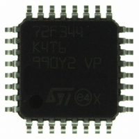
ST72F344K4T6 STMicroelectronics, ST72F344K4T6 Datasheet - Page 105

ST72F344K4T6
Manufacturer Part Number
ST72F344K4T6
Description
MCU 8BIT 16KB FLASH MEM 32-LQFP
Manufacturer
STMicroelectronics
Series
ST7r
Datasheet
1.ST72F344K2T6.pdf
(247 pages)
Specifications of ST72F344K4T6
Core Processor
ST7
Core Size
8-Bit
Speed
8MHz
Connectivity
I²C, LIN, SCI, SPI
Peripherals
LVD, POR, PWM, WDT
Number Of I /o
24
Program Memory Size
16KB (16K x 8)
Program Memory Type
FLASH
Eeprom Size
256 x 8
Ram Size
1K x 8
Voltage - Supply (vcc/vdd)
2.7 V ~ 5.5 V
Data Converters
A/D 12x10b
Oscillator Type
Internal
Operating Temperature
-40°C ~ 85°C
Package / Case
32-LQFP
Processor Series
ST72F3x
Core
ST7
Data Bus Width
8 bit
Data Ram Size
1 KB
Interface Type
I2C, SCI, SPI
Maximum Clock Frequency
8 MHz
Number Of Programmable I/os
34
Number Of Timers
2
Maximum Operating Temperature
+ 85 C
Mounting Style
SMD/SMT
Development Tools By Supplier
ST72F34X-SK/RAIS, ST7MDT40-EMU3, STX-RLINK
Minimum Operating Temperature
- 40 C
On-chip Adc
10 bit, 8 Channel
For Use With
497-5046 - KIT TOOL FOR ST7/UPSD/STR7 MCU
Lead Free Status / RoHS Status
Lead free / RoHS Compliant
Other names
497-5611
Available stocks
Company
Part Number
Manufacturer
Quantity
Price
Company:
Part Number:
ST72F344K4T6
Manufacturer:
STMicroelectronics
Quantity:
10 000
Company:
Part Number:
ST72F344K4T6TR
Manufacturer:
STMicroelectronics
Quantity:
10 000
- Current page: 105 of 247
- Download datasheet (3Mb)
ST72344xx ST72345xx
Note:
Figure 54. Pulse width modulation mode timing example
1. OC1R = 2ED0h, OC2R = 34E2, OLVL1 = 0, OLVL2 = 1
Pulse-width modulation mode
Pulse-width modulation (PWM) mode enables the generation of a signal with a frequency
and pulse length determined by the value of the OC1R and OC2R registers.
Pulse-width modulation mode uses the complete Output Compare 1 function plus the OC2R
register, and so this functionality can not be used when PWM mode is activated.
In PWM mode, double buffering is implemented on the output compare registers. Any new
values written in the OC1R and OC2R registers are loaded in their respective shadow
registers (double buffer) only at the end of the PWM period (OC2) to avoid spikes on the
PWM output pin (OCMP1). The shadow registers contain the reference values for
comparison in PWM “double buffering” mode.
There is a locking mechanism for transferring the OCiR value to the buffer. After a write to
the OCiHR register, transfer of the new compare value to the buffer is inhibited until OCiLR
is also written.
Unlike in Output Compare mode, the compare function is always enabled in PWM mode.
Procedure:
To use pulse-width modulation mode:
1.
2.
3.
4.
Load the OC2R register with the value corresponding to the period of the signal using
the formula in the opposite column.
Load the OC1R register with the value corresponding to the period of the pulse if
(OLVL1=0 and OLVL2=1) using the formula in the opposite column.
Select the following in the CR1 register:
–
–
Select the following in the CR2 register:
–
–
–
COUNTER 34E2
Using the OLVL1 bit, select the level to be applied to the OCMP1 pin after a
successful comparison with OC1R register.
Using the OLVL2 bit, select the level to be applied to the OCMP1 pin after a
successful comparison with OC2R register.
Set OC1E bit: the OCMP1 pin is then dedicated to the output compare 1 function.
Set the PWM bit.
Select the timer clock (CC[1:0]) (see
OCMP1
compare2
FFFC FFFD FFFE
Doc ID 12321 Rev 5
OLVL2
Table 50: Clock control
compare1
2ED0 2ED1 2ED2
OLVL1
bits).
On-chip peripherals
compare2
34E2
OLVL2
FFFC
105/247
Related parts for ST72F344K4T6
Image
Part Number
Description
Manufacturer
Datasheet
Request
R

Part Number:
Description:
STMicroelectronics [RIPPLE-CARRY BINARY COUNTER/DIVIDERS]
Manufacturer:
STMicroelectronics
Datasheet:

Part Number:
Description:
STMicroelectronics [LIQUID-CRYSTAL DISPLAY DRIVERS]
Manufacturer:
STMicroelectronics
Datasheet:

Part Number:
Description:
BOARD EVAL FOR MEMS SENSORS
Manufacturer:
STMicroelectronics
Datasheet:

Part Number:
Description:
NPN TRANSISTOR POWER MODULE
Manufacturer:
STMicroelectronics
Datasheet:

Part Number:
Description:
TURBOSWITCH ULTRA-FAST HIGH VOLTAGE DIODE
Manufacturer:
STMicroelectronics
Datasheet:

Part Number:
Description:
Manufacturer:
STMicroelectronics
Datasheet:

Part Number:
Description:
DIODE / SCR MODULE
Manufacturer:
STMicroelectronics
Datasheet:

Part Number:
Description:
DIODE / SCR MODULE
Manufacturer:
STMicroelectronics
Datasheet:

Part Number:
Description:
Search -----> STE16N100
Manufacturer:
STMicroelectronics
Datasheet:

Part Number:
Description:
Search ---> STE53NA50
Manufacturer:
STMicroelectronics
Datasheet:

Part Number:
Description:
NPN Transistor Power Module
Manufacturer:
STMicroelectronics
Datasheet:

Part Number:
Description:
DIODE / SCR MODULE
Manufacturer:
STMicroelectronics
Datasheet:


