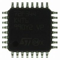
ST72F344K4T6 STMicroelectronics, ST72F344K4T6 Datasheet - Page 155

ST72F344K4T6
Manufacturer Part Number
ST72F344K4T6
Description
MCU 8BIT 16KB FLASH MEM 32-LQFP
Manufacturer
STMicroelectronics
Series
ST7r
Datasheet
1.ST72F344K2T6.pdf
(247 pages)
Specifications of ST72F344K4T6
Core Processor
ST7
Core Size
8-Bit
Speed
8MHz
Connectivity
I²C, LIN, SCI, SPI
Peripherals
LVD, POR, PWM, WDT
Number Of I /o
24
Program Memory Size
16KB (16K x 8)
Program Memory Type
FLASH
Eeprom Size
256 x 8
Ram Size
1K x 8
Voltage - Supply (vcc/vdd)
2.7 V ~ 5.5 V
Data Converters
A/D 12x10b
Oscillator Type
Internal
Operating Temperature
-40°C ~ 85°C
Package / Case
32-LQFP
Processor Series
ST72F3x
Core
ST7
Data Bus Width
8 bit
Data Ram Size
1 KB
Interface Type
I2C, SCI, SPI
Maximum Clock Frequency
8 MHz
Number Of Programmable I/os
34
Number Of Timers
2
Maximum Operating Temperature
+ 85 C
Mounting Style
SMD/SMT
Development Tools By Supplier
ST72F34X-SK/RAIS, ST7MDT40-EMU3, STX-RLINK
Minimum Operating Temperature
- 40 C
On-chip Adc
10 bit, 8 Channel
For Use With
497-5046 - KIT TOOL FOR ST7/UPSD/STR7 MCU
Lead Free Status / RoHS Status
Lead free / RoHS Compliant
Other names
497-5611
Available stocks
Company
Part Number
Manufacturer
Quantity
Price
Company:
Part Number:
ST72F344K4T6
Manufacturer:
STMicroelectronics
Quantity:
10 000
Company:
Part Number:
ST72F344K4T6TR
Manufacturer:
STMicroelectronics
Quantity:
10 000
ST72344xx ST72345xx
Note:
Note:
In 10-bit addressing mode, to switch the master to Receiver mode, software must generate
a repeated Start condition and resend the header sequence with the least significant bit set
(11110xx1).
Master receiver
Following the address transmission and after SR1 and CR registers have been accessed,
the master receives bytes from the SDA line into the DR register via the internal shift
register. After each byte the interface generates in sequence:
●
●
Then the interface waits for a read of the SR1 register followed by a read of the DR register,
holding the SCL line low (see
To close the communication: before reading the last byte from the DR register, set the STOP
bit to generate the Stop condition. The interface goes automatically back to slave mode
(M/SL bit cleared).
In order to generate the non-acknowledge pulse after the last received data byte, the ACK
bit must be cleared just before reading the second last data byte.
Master transmitter
Following the address transmission and after SR1 register has been read, the master sends
bytes from the DR register to the SDA line via the internal shift register.
The master waits for a read of the SR1 register followed by a write in the DR register,
holding the SCL line low (see
When the acknowledge bit is received, the interface sets:
●
To close the communication: after writing the last byte to the DR register, set the STOP bit to
generate the Stop condition. The interface goes automatically back to slave mode (M/SL bit
cleared).
Error cases
●
Acknowledge pulse if the ACK bit is set
EVF and BTF bits are set by hardware with an interrupt if the ITE bit is set.
EVF and BTF bits with an interrupt if the ITE bit is set.
BERR: Detection of a Stop or a Start condition during a byte transfer. In this case, the
EVF and BERR bits are set by hardware with an interrupt if ITE is set.
Note that BERR will not be set if an error is detected during the first pulse of each 9-bit
transaction:
Single Master Mode
If a Start or Stop is issued during the first pulse of a 9-bit transaction, the BERR flag will
not be set and transfer will continue however the BUSY flag will be reset. To work
around this, slave devices should issue a NACK when they receive a misplaced Start or
Stop. The reception of a NACK or BUSY by the master in the middle of communication
gives the possibility to re-initiate transmission.
Multimaster Mode
Normally the BERR bit would be set whenever unauthorized transmission takes place
while transfer is already in progress. However, an issue will arise if an external master
generates an unauthorized Start or Stop while the I
9-bit transaction. It is possible to work around this by polling the BUSY bit during I
Doc ID 12321 Rev 5
Figure 69
Figure 69
Transfer sequencing EV7).
Transfer sequencing EV8).
2
C master is on the first pulse of a
On-chip peripherals
155/247
2
C


