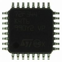
ST72F344K4T6 STMicroelectronics, ST72F344K4T6 Datasheet - Page 170

ST72F344K4T6
Manufacturer Part Number
ST72F344K4T6
Description
MCU 8BIT 16KB FLASH MEM 32-LQFP
Manufacturer
STMicroelectronics
Series
ST7r
Datasheet
1.ST72F344K2T6.pdf
(247 pages)
Specifications of ST72F344K4T6
Core Processor
ST7
Core Size
8-Bit
Speed
8MHz
Connectivity
I²C, LIN, SCI, SPI
Peripherals
LVD, POR, PWM, WDT
Number Of I /o
24
Program Memory Size
16KB (16K x 8)
Program Memory Type
FLASH
Eeprom Size
256 x 8
Ram Size
1K x 8
Voltage - Supply (vcc/vdd)
2.7 V ~ 5.5 V
Data Converters
A/D 12x10b
Oscillator Type
Internal
Operating Temperature
-40°C ~ 85°C
Package / Case
32-LQFP
Processor Series
ST72F3x
Core
ST7
Data Bus Width
8 bit
Data Ram Size
1 KB
Interface Type
I2C, SCI, SPI
Maximum Clock Frequency
8 MHz
Number Of Programmable I/os
34
Number Of Timers
2
Maximum Operating Temperature
+ 85 C
Mounting Style
SMD/SMT
Development Tools By Supplier
ST72F34X-SK/RAIS, ST7MDT40-EMU3, STX-RLINK
Minimum Operating Temperature
- 40 C
On-chip Adc
10 bit, 8 Channel
For Use With
497-5046 - KIT TOOL FOR ST7/UPSD/STR7 MCU
Lead Free Status / RoHS Status
Lead free / RoHS Compliant
Other names
497-5611
Available stocks
Company
Part Number
Manufacturer
Quantity
Price
Company:
Part Number:
ST72F344K4T6
Manufacturer:
STMicroelectronics
Quantity:
10 000
Company:
Part Number:
ST72F344K4T6TR
Manufacturer:
STMicroelectronics
Quantity:
10 000
On-chip peripherals
170/247
The Byte count register is reset when it reaches 256 bytes, whatever the page length, for all
slave addresses, including slave 3.
DMA
The I
A DMA request is issued to the DMA controller on reception of a byte or just before
transmission of a byte.
When a byte is written by DMA in RAM, the CPU is stalled for max. 2 cycles. When several
bytes are transferred from the I2C bus to RAM, the DMA releases between each byte and
the CPU resumes processing until the DMA writes the next byte.
RAM buffer write protection
By setting the WP1/WP2 bits in the I2C3SCR2 register it is possible to protect the RAM
buffer of Slaves 1/2 respectively against write access from the master.
If a write operation is attempted, the slave address is acknowledged, the current address
register is overwritten, data is also acknowledged but it is not written to the RAM. Both the
current address and byte count registers are incremented as in normal operation.
In case of write access to a write protected address, no interrupt is generated and the
BusyW bit in the I2C3SCR2 register is not set.
Only write operations are disabled/enabled. Read operations are not affected.
Byte-pair coherency for I
Byte-pair coherency allows the I
corrupted by a simultaneous CPU update. Two mechanisms are implemented, covering the
two possible cases:
1.
2.
CPU updates a word in RAM after the first byte has been transferred to the I2C shift
register from RAM. In this case, the first byte read from RAM would be the MSB of the
old word and 2nd byte would be the LSB of the new word.
To prevent this corruption, the I2C3S uses DMA to systematically read a 2-byte word
when it receives a read command from the I
at address 2n. Using DMA, the MSB is moved from RAM address 2n to the I2C shift
register and the LSB from RAM address 2n+1 moved to a shadow register in the I2C3S
peripheral. The CPU is stalled for a maximum of 2 cycles during word transfer.
In case only one byte is read, the unused content of the shadow register will be
automatically overwritten when a new read operation is performed.
In case a second byte is read in the same I
the content of the shadow register is transferred to the shift register and transmitted to
the master.
This process continues until a Stop or Restart condition occurs.
I2C3S attempts to read a word while the CPU is updating the RAM buffer. To prevent
data corruption, the CPU must switch operation to Word mode prior to updating a word
in the RAM buffer. Word mode is enabled by software using the B/W bit in the
I2C3SCR2 register. In Word mode, when the CPU writes the MSB of a word to address
2n, it is stored in a shadow register rather than being actually written in RAM. When the
CPU writes the second byte (the LSB) at address 2n+1, it is directly written in RAM.
The next cycle after the write to address 2n+1, the MSB is automatically written from
the shadow register to RAM address 2n. DMA is disabled for a 1 cycle while the CPU is
writing a word.
2
C slaves use a DMA controller to write/read data to/from their RAM buffer.
2
C read operations
Doc ID 12321 Rev 5
2
C master to read a 16-bit word and ensures that it is not
2
2
C message (no Stop or Restart condition)
C master. The MSB of the word should be
ST72344xx ST72345xx


