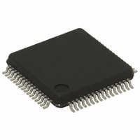
STR752FR2T6 STMicroelectronics, STR752FR2T6 Datasheet - Page 58

STR752FR2T6
Manufacturer Part Number
STR752FR2T6
Description
MCU 32BIT 256KB FLASH 64-LQFP
Manufacturer
STMicroelectronics
Series
STR7r
Datasheet
1.STR750FV0T6.pdf
(84 pages)
Specifications of STR752FR2T6
Core Processor
ARM7
Core Size
32-Bit
Speed
60MHz
Connectivity
CAN, I²C, SPI, SSI, SSP, UART/USART
Peripherals
DMA, PWM, WDT
Number Of I /o
38
Program Memory Size
256KB (256K x 8)
Program Memory Type
FLASH
Ram Size
16K x 8
Voltage - Supply (vcc/vdd)
3 V ~ 5.5 V
Data Converters
A/D 11x10b
Oscillator Type
Internal
Operating Temperature
-40°C ~ 85°C
Package / Case
64-LQFP
Processor Series
STR752x
Core
ARM7TDMI
Data Bus Width
32 bit
Data Ram Size
16 KB
Interface Type
CAN, I2C, SPI, SSI, SSP, USB
Maximum Clock Frequency
60 MHz
Number Of Programmable I/os
38
Number Of Timers
6
Maximum Operating Temperature
+ 85 C
Mounting Style
SMD/SMT
3rd Party Development Tools
EWARM, EWARM-BL, KSDK-STR750-PLUS, MCBSTR750, MCBSTR750U, MCBSTR750UME, MDK-ARM, RL-ARM, ULINK2
Development Tools By Supplier
STR750-MCKIT, STR750-SK/HIT, STR750-SK/IAR, STR750-SK/KEIL, STR750-SK/RAIS, STR750-EVAL, STX-PRO/RAIS, STX-RLINK, STR79-RVDK/CPP, STR79-RVDK, STR79-RVDK/UPG
Minimum Operating Temperature
- 40 C
On-chip Adc
10 bit, 11 Channel
For Use With
MCBSTR750UME - BOARD EVAL MCBSTR750 + ULINK-MEMCBSTR750U - BOARD EVAL MCBSTR750 + ULINK2497-5754 - KIT STARTER IAR STR750497-5753 - KIT STARTER KEIL FOR STR7/STR9497-5752 - KIT STARTER IAR FOR STR7/STR9497-5748 - BOARD EVALUATION FOR STR750XF497-5046 - KIT TOOL FOR ST7/UPSD/STR7 MCU
Lead Free Status / RoHS Status
Lead free / RoHS Compliant
Eeprom Size
-
Lead Free Status / Rohs Status
Details
Other names
497-5653
Available stocks
Company
Part Number
Manufacturer
Quantity
Price
Company:
Part Number:
STR752FR2T6
Manufacturer:
STM
Quantity:
6 600
Company:
Part Number:
STR752FR2T6
Manufacturer:
STMicroelectronics
Quantity:
10 000
Electrical parameters
58/84
NRSTIN and NRSTOUT pins
NRSTIN Pin Input Driver is TTL/LVTTL as for all GP I/Os. A permanent pull-up is present
which is the same as R
NRSTOUT Pin Output Driver is equivalent to the O2 type driver except that it works only as
an open-drain (the P-MOS is de-activated). A permanent pull-up is present which is the
same as R
Subject to general operating conditions for V
Table 35. NRSTIN and NRSTOUT pins
1. Data based on product characterisation, not tested in production.
2. Hysteresis voltage between Schmitt trigger switching levels.
3. The I
4. The R
5. To guarantee the reset of the device, a minimum pulse of 15 µs has to be applied to the internal reset. At
6. The reset network (the resistor and two capacitors) protects the device against parasitic resets, especially
7. In fact the filter is made to ignore all incoming pulses with short duration:
V
R
V
V
V
t
hys(NRSTIN)
OL(NRSTIN)
w(RSTL)out
t
t
PU(NRSTIN)
sum of I
V
is established, an external reset pulse will be internally stretched up to 15 µs thanks to the reset pulse
stretcher.
in noisy environments.
- all negative spikes with a duration less than 150 ns are filtered
- all trains of negative spikes with a ratio of 1/2 are filtered. This means that all spikes with a maximum
duration of 150 ns with minimum interval between spikes of 75 ns are filtered.
Data guaranteed by design, not tested in production.
Symbol
IH(NRSTIN)
IL(NRSTIN)
h(RSTL)in
g(RSTL)in
DD_IO
IO
PU
power-up, the built-in reset stretcher may not generate the 15 µs pulse duration while once V
current sunk must always respect the absolute maximum rating specified in
IO
pull-up equivalent resistor are based on a resistive transistor
PU
(I/O ports and control pins) must not exceed I
(see
NRSTIN Input low level
voltage
NRSTIN Input high level
voltage
NRSTIN Schmitt trigger
voltage hysteresis
NRSTOUT Output low level
voltage
NRSTIN Weak pull-up
equivalent resistor
Generated reset pulse
duration (visible at NRSTOUT
pin)
External reset pulse hold time
at NRSTIN pin
maximum negative spike
duration filtered at NRSTIN
pin
(7)
(5)
: General characteristics on page
(1)
(1)
(3)
PU
Parameter
(see
(6)
(2)
(4)
: General characteristics on page
STR750Fxx STR751Fxx STR752Fxx STR755Fxx
I
V
Internal reset source
At V
When V
established
The time between two
spikes must be higher
than 1/2 of the spike
duration.
IO
DD_IO
IN
=+2 mA
=
DD_IO
V
VSS
SS
Conditions
and T
DD_IO
.
54)
power-up
V
V
(5)
DD_IO
DD_IO
A
is
unless otherwise specified.
=3.3 V
=5 V
(5)
54)
Min Typ
25
20
15
20
2
1
Section 6.2.2
400
150
50
31
20
1)
Max Unit
100
100
0.8
0.4
and the
DD_IO
mV
kΩ
kΩ
μs
μs
μs
ns
V
V


