STR752FR2T6 STMicroelectronics, STR752FR2T6 Datasheet - Page 6
STR752FR2T6
Manufacturer Part Number
STR752FR2T6
Description
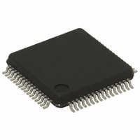
MCU 32BIT 256KB FLASH 64-LQFP
Manufacturer
STMicroelectronics
Series
STR7r
Datasheet
1.STR750FV0T6.pdf
(84 pages)
Specifications of STR752FR2T6
Core Processor
ARM7
Core Size
32-Bit
Speed
60MHz
Connectivity
CAN, I²C, SPI, SSI, SSP, UART/USART
Peripherals
DMA, PWM, WDT
Number Of I /o
38
Program Memory Size
256KB (256K x 8)
Program Memory Type
FLASH
Ram Size
16K x 8
Voltage - Supply (vcc/vdd)
3 V ~ 5.5 V
Data Converters
A/D 11x10b
Oscillator Type
Internal
Operating Temperature
-40°C ~ 85°C
Package / Case
64-LQFP
Processor Series
STR752x
Core
ARM7TDMI
Data Bus Width
32 bit
Data Ram Size
16 KB
Interface Type
CAN, I2C, SPI, SSI, SSP, USB
Maximum Clock Frequency
60 MHz
Number Of Programmable I/os
38
Number Of Timers
6
Maximum Operating Temperature
+ 85 C
Mounting Style
SMD/SMT
3rd Party Development Tools
EWARM, EWARM-BL, KSDK-STR750-PLUS, MCBSTR750, MCBSTR750U, MCBSTR750UME, MDK-ARM, RL-ARM, ULINK2
Development Tools By Supplier
STR750-MCKIT, STR750-SK/HIT, STR750-SK/IAR, STR750-SK/KEIL, STR750-SK/RAIS, STR750-EVAL, STX-PRO/RAIS, STX-RLINK, STR79-RVDK/CPP, STR79-RVDK, STR79-RVDK/UPG
Minimum Operating Temperature
- 40 C
On-chip Adc
10 bit, 11 Channel
For Use With
MCBSTR750UME - BOARD EVAL MCBSTR750 + ULINK-MEMCBSTR750U - BOARD EVAL MCBSTR750 + ULINK2497-5754 - KIT STARTER IAR STR750497-5753 - KIT STARTER KEIL FOR STR7/STR9497-5752 - KIT STARTER IAR FOR STR7/STR9497-5748 - BOARD EVALUATION FOR STR750XF497-5046 - KIT TOOL FOR ST7/UPSD/STR7 MCU
Lead Free Status / RoHS Status
Lead free / RoHS Compliant
Eeprom Size
-
Lead Free Status / Rohs Status
Details
Other names
497-5653
Available stocks
Company
Part Number
Manufacturer
Quantity
Price
Company:

Part Number:
STR752FR2T6
Manufacturer:
STM
Quantity:
6 600
Company:
Part Number:
STR752FR2T6
Manufacturer:
STMicroelectronics
Quantity:
10 000


Introduction
6/84
Serial memory interface (SMI)
The Serial Memory interface is directly able to access up to 4 serial FLASH devices. It can
be used to access data, execute code directly or boot the application from external memory.
The memory is addressed as 4 banks of up to 16 Mbytes each.
Clocks and start-up
After RESET or when exiting from Low Power Mode, the CPU is clocked immediately by an
internal RC oscillator (FREEOSC) at a frequency centered around 5 MHz, so the application
code can start executing without delay. In parallel, the 4/8 MHz Oscillator is enabled and its
stabilization time is monitored using a dedicated counter.
An oscillator failure detection is implemented: when the clock disappears on the XT1 pin, the
circuit automatically switches to the FREEOSC oscillator and an interrupt is generated.
In Run mode, the AHB and APB clock speeds can be set at a large number of different
frequencies thanks to the PLL and various prescalers: up to 60 MHz for AHB and up to 32
MHz for APB when fetching from Flash (64 MHz and 32 MHz when fetching from SRAM).
In SLOW mode, the AHB clock can be significantly decreased to reduce power
consumption.
The built-in Clock Controller also provides the 48 MHz USB clock directly without any extra
oscillators or PLL. For instance, starting from the 4 MHz crystal source, it is possible to
obtain in parallel 60 MHz for the AHB clock, 48 MHz for the USB clock and 30 MHz for the
APB peripherals.
Boot modes
At start-up, boot pins are used to select one of five boot options:
●
●
●
●
Booting from SMI memory allows booting from a serial flash. This way, a specific boot
monitor can be implemented. Alternatively, the STR750F can boot from the internal boot
loader that implements a boot from UART.
Power supply schemes
You can connect the device in any of the following ways depending on your application.
●
●
●
Boot from internal flash
Boot from external serial Flash memory
Boot from internal boot loader
Boot from internal SRAM
Power Scheme 1: Single external 3.3V power source. In this configuration the
V
regulator and the V
regulator. This scheme has the advantage of requiring only one 3.3V power source.
Power Scheme 2: Dual external 3.3V and 1.8V power sources. In this configuration,
the internal voltage regulators are switched off by forcing the VREG_DIS pin to high
level. V
V
for applications which already provide an 1.8V power supply.
Power Scheme 3: Single external 5.0V power source. In this configuration the
V
CORE
BACKUP
CORE
supply required for the internal logic is generated internally by the main voltage
supply required for the internal logic is generated internally by the main voltage
CORE
through the V
is provided externally through the V
BACKUP
18_BKP
supply is generated internally by the low power voltage
pin. This scheme is intended to save power consumption
STR750Fxx STR751Fxx STR752Fxx STR755Fxx
18
and V
18REG
power pins and
Related parts for STR752FR2T6
Image
Part Number
Description
Manufacturer
Datasheet
Request
R

Part Number:
Description:
IC MCU ARM7 TDMI 256K 144TQFP
Manufacturer:
STMicroelectronics
Datasheet:

Part Number:
Description:
MCU 32BIT 256KB FLASH 100-LQFP
Manufacturer:
STMicroelectronics
Datasheet:

Part Number:
Description:
IC MCU ARM7 TDMI 256K 64-LQFP
Manufacturer:
STMicroelectronics
Datasheet:
Part Number:
Description:
MCU 32BIT 64KB FLASH 64-LQFP
Manufacturer:
STMicroelectronics
Datasheet:
Part Number:
Description:
IC MCU ARM7 TDMI 128K 64-LQFP
Manufacturer:
STMicroelectronics
Datasheet:

Part Number:
Description:
MCU ARM7 32BIT 64-LFBGA
Manufacturer:
STMicroelectronics
Datasheet:

Part Number:
Description:
MCU 32BIT 128K FLASH 100-TQFP
Manufacturer:
STMicroelectronics
Datasheet:
Part Number:
Description:
IC MCU ARM7 128K FLASH 100-TQFP
Manufacturer:
STMicroelectronics
Datasheet:
Part Number:
Description:
MCU 32BIT 128KB FLASH 100-LQFP
Manufacturer:
STMicroelectronics
Datasheet:
Part Number:
Description:
MCU 32BIT 256KB FLASH 100-TQFP
Manufacturer:
STMicroelectronics
Datasheet:
Part Number:
Description:
IC MCU ARM7 TDMI 256K 64-LQFP
Manufacturer:
STMicroelectronics
Datasheet:

Part Number:
Description:
MCU 32BIT 256KB FLASH 144-LQFP
Manufacturer:
STMicroelectronics
Datasheet:

Part Number:
Description:
MCU 32BIT 256KB FLASH 144-LFBGA
Manufacturer:
STMicroelectronics
Datasheet:
Part Number:
Description:
IC MCU ARM7 256K FLASH 100-TQFP
Manufacturer:
STMicroelectronics
Datasheet:
Part Number:
Description:
MCU 32BIT 256KB FLASH 144-LQFP
Manufacturer:
STMicroelectronics
Datasheet: