HD6417034AFI20V Renesas Electronics America, HD6417034AFI20V Datasheet - Page 391
HD6417034AFI20V
Manufacturer Part Number
HD6417034AFI20V
Description
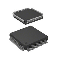
MCU 5V 0K I-TEMP PB-FREE 112-QFP
Manufacturer
Renesas Electronics America
Series
SuperH® SH7030r
Datasheet
1.HD6417034AFI20.pdf
(689 pages)
Specifications of HD6417034AFI20V
Core Processor
SH-1
Core Size
32-Bit
Speed
20MHz
Connectivity
EBI/EMI, SCI
Peripherals
DMA, POR, PWM, WDT
Number Of I /o
32
Program Memory Type
ROMless
Ram Size
4K x 8
Voltage - Supply (vcc/vdd)
4.5 V ~ 5.5 V
Data Converters
A/D 8x10b
Oscillator Type
Internal
Operating Temperature
-20°C ~ 75°C
Package / Case
112-QFP
Lead Free Status / RoHS Status
Lead free / RoHS Compliant
Eeprom Size
-
Program Memory Size
-
Available stocks
Company
Part Number
Manufacturer
Quantity
Price
Company:

Part Number:
HD6417034AFI20V
Manufacturer:
Renesas Electronics America
Quantity:
10 000


(SMR) before setting CKE1 and CKE0. For further details on selection of the SCI clock source,
see table 13.9 in section 13.3, Operation.
Bit 1:
CKE1
0
0
1
1
Notes: 1. The SCK pin is multiplexed with other functions. Set the pin function controller (PFC) to
13.2.7
The serial status register (SSR) is an 8-bit register containing multiprocessor bit values, and status
flags that indicate the SCI operating status.
The CPU can always read and write to SSR, but cannot write 1 in the status flags (TDRE, RDRF,
ORER, PER, and FER). These flags can be cleared to 0 only if they have first been read (after
being set to 1). Bits 2 (TEND) and 1 (MPB) are read-only bits that cannot be written. SSR is
initialized to H'84 by a reset and in standby mode.
Note: * Only 0 can be written, to clear the flag.
Bit
Initial value
Read/Write
2. Initial value
3. The output clock frequency is the same as the bit rate.
4. The input clock frequency is 16 times the bit rate.
Bit 0:
CKE0
0
1
0
1
Serial Status Register
select the SCK function and SCK input/output for the SCK pin.
Description *
Asynchronous mode
Synchronous mode
Asynchronous mode
Synchronous mode
Asynchronous mode
Synchronous mode
Asynchronous mode
Synchronous mode
R/(W)*
TDRE
7
1
1
R/(W)*
RDRF
6
0
R/(W)*
ORER
Internal clock, SCK pin used for input pin (input signal
is ignored) or output pin (output level is undefined) *
Internal clock, SCK pin used for serial clock output *
Internal clock, SCK pin used for clock output *
Internal clock, SCK pin used for serial clock output
External clock, SCK pin used for clock input *
External clock, SCK pin used for serial clock input
External clock, SCK pin used for clock input *
External clock, SCK pin used for serial clock input
5
0
Section 13 Serial Communication Interface (SCI)
R/(W)*
FER
4
0
Rev. 7.00 Jan 31, 2006 page 363 of 658
R/(W)*
PER
3
0
TEND
R
2
1
REJ09B0272-0700
MPB
R
1
0
(Initial value)
(Initial value)
4
4
3
MPBT
R/W
0
0
2
2
Related parts for HD6417034AFI20V
Image
Part Number
Description
Manufacturer
Datasheet
Request
R

Part Number:
Description:
KIT STARTER FOR M16C/29
Manufacturer:
Renesas Electronics America
Datasheet:

Part Number:
Description:
KIT STARTER FOR R8C/2D
Manufacturer:
Renesas Electronics America
Datasheet:

Part Number:
Description:
R0K33062P STARTER KIT
Manufacturer:
Renesas Electronics America
Datasheet:

Part Number:
Description:
KIT STARTER FOR R8C/23 E8A
Manufacturer:
Renesas Electronics America
Datasheet:

Part Number:
Description:
KIT STARTER FOR R8C/25
Manufacturer:
Renesas Electronics America
Datasheet:

Part Number:
Description:
KIT STARTER H8S2456 SHARPE DSPLY
Manufacturer:
Renesas Electronics America
Datasheet:

Part Number:
Description:
KIT STARTER FOR R8C38C
Manufacturer:
Renesas Electronics America
Datasheet:

Part Number:
Description:
KIT STARTER FOR R8C35C
Manufacturer:
Renesas Electronics America
Datasheet:

Part Number:
Description:
KIT STARTER FOR R8CL3AC+LCD APPS
Manufacturer:
Renesas Electronics America
Datasheet:
Part Number:
Description:
KIT STARTER FOR RX610
Manufacturer:
Renesas Electronics America
Datasheet:

Part Number:
Description:
KIT STARTER FOR R32C/118
Manufacturer:
Renesas Electronics America
Datasheet:

Part Number:
Description:
KIT DEV RSK-R8C/26-29
Manufacturer:
Renesas Electronics America
Datasheet:

Part Number:
Description:
KIT STARTER FOR SH7124
Manufacturer:
Renesas Electronics America
Datasheet:

Part Number:
Description:
KIT STARTER FOR H8SX/1622
Manufacturer:
Renesas Electronics America
Datasheet:

Part Number:
Description:
KIT DEV FOR SH7203
Manufacturer:
Renesas Electronics America
Datasheet: