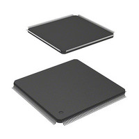
HD6417705F133BV Renesas Electronics America, HD6417705F133BV Datasheet - Page 321

HD6417705F133BV
Manufacturer Part Number
HD6417705F133BV
Description
MPU 3V 0K PB-FREE 208 FP
Manufacturer
Renesas Electronics America
Series
SuperH® SH7700r
Datasheet
1.HD6417705F133BV.pdf
(741 pages)
Specifications of HD6417705F133BV
Core Processor
SH-3
Core Size
32-Bit
Speed
133MHz
Connectivity
EBI/EMI, FIFO, IrDA, SCI, USB
Peripherals
DMA, POR, PWM, WDT
Number Of I /o
105
Program Memory Type
ROMless
Ram Size
32K x 8
Voltage - Supply (vcc/vdd)
1.4 V ~ 1.6 V
Data Converters
A/D 4x10b
Oscillator Type
Internal
Operating Temperature
-20°C ~ 75°C
Package / Case
208-LQFP
Lead Free Status / RoHS Status
Lead free / RoHS Compliant
Eeprom Size
-
Program Memory Size
-
- Current page: 321 of 741
- Download datasheet (5Mb)
The clock pulse generator blocks function as follows:
1. PLL Circuit 1
2. PLL Circuit 2
3. Crystal Oscillator
4. Divider 1
5. Clock Frequency Control Circuit
6. Standby Control Circuit
7. Frequency Control Register
8. Standby Control Register
9. USB Clock Control Register
PLL circuit 1 doubles, triples, quadruples, or leaves unchanged the input clock frequency from
the CKIO pin or PLL circuit 2. The multiplication rate is set by the frequency control register.
When this is done, the phase of the rising edge of the internal clock is controlled so that it will
synchronize with the phase of the rising edge of the CKIO pin.
PLL circuit 2 leaves unchanged, doubles, or quadruples the input clock frequency coming from
the crystal oscillator or EXTAL pin. The multiplication ratio is fixed by the clock-operating
mode. The clock-operating mode is set by pins MD0, MD1, and MD2. For more details on
clock operating modes, refer to table 9.2.
This oscillator circuit is used when a crystal resonator is connected to the XTAL and EXTAL
pins. This crystal oscillator operates according to the clock operating mode setting.
Divider 1 generates a clock at the operating frequency used by the internal or peripheral clock.
The operating frequency can be 1, 1/2, 1/3, or 1/4 times the output frequency of PLL circuit 1,
as long as it stays at or above the clock frequency of the CKIO pin. The division ratio is set in
the frequency control register.
The clock frequency control circuit controls the clock frequency using the MD0, MD1, and
MD2 pins and the frequency control register.
The standby control circuit controls the state of the on-chip oscillator and other modules during
clock switching and software/standby modes.
The frequency control register has control bits assigned for the following functions: clock
output/non-output from the CKIO pin, the frequency multiplication ratio of PLL circuit 1, and
the frequency division ratio of the internal clock and the peripheral clock.
The standby control register has bits for controlling the power-down modes. See section 11,
Power-Down Modes, for more information.
The source clock generating the USB clock is set in the USB clock control register.
Rev. 2.00, 09/03, page 273 of 690
Related parts for HD6417705F133BV
Image
Part Number
Description
Manufacturer
Datasheet
Request
R

Part Number:
Description:
KIT STARTER FOR M16C/29
Manufacturer:
Renesas Electronics America
Datasheet:

Part Number:
Description:
KIT STARTER FOR R8C/2D
Manufacturer:
Renesas Electronics America
Datasheet:

Part Number:
Description:
R0K33062P STARTER KIT
Manufacturer:
Renesas Electronics America
Datasheet:

Part Number:
Description:
KIT STARTER FOR R8C/23 E8A
Manufacturer:
Renesas Electronics America
Datasheet:

Part Number:
Description:
KIT STARTER FOR R8C/25
Manufacturer:
Renesas Electronics America
Datasheet:

Part Number:
Description:
KIT STARTER H8S2456 SHARPE DSPLY
Manufacturer:
Renesas Electronics America
Datasheet:

Part Number:
Description:
KIT STARTER FOR R8C38C
Manufacturer:
Renesas Electronics America
Datasheet:

Part Number:
Description:
KIT STARTER FOR R8C35C
Manufacturer:
Renesas Electronics America
Datasheet:

Part Number:
Description:
KIT STARTER FOR R8CL3AC+LCD APPS
Manufacturer:
Renesas Electronics America
Datasheet:

Part Number:
Description:
KIT STARTER FOR RX610
Manufacturer:
Renesas Electronics America
Datasheet:

Part Number:
Description:
KIT STARTER FOR R32C/118
Manufacturer:
Renesas Electronics America
Datasheet:

Part Number:
Description:
KIT DEV RSK-R8C/26-29
Manufacturer:
Renesas Electronics America
Datasheet:

Part Number:
Description:
KIT STARTER FOR SH7124
Manufacturer:
Renesas Electronics America
Datasheet:

Part Number:
Description:
KIT STARTER FOR H8SX/1622
Manufacturer:
Renesas Electronics America
Datasheet:

Part Number:
Description:
KIT DEV FOR SH7203
Manufacturer:
Renesas Electronics America
Datasheet:


