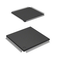
DF2166VTE33 Renesas Electronics America, DF2166VTE33 Datasheet - Page 189

DF2166VTE33
Manufacturer Part Number
DF2166VTE33
Description
MCU FLASH 3V 512K 33MHZ 144TQFP
Manufacturer
Renesas Electronics America
Series
H8® H8S/2100r
Datasheet
1.HS2168EPI61H-U.pdf
(876 pages)
Specifications of DF2166VTE33
Core Processor
H8S/2000
Core Size
16-Bit
Speed
33MHz
Connectivity
I²C, IrDA, LPC, SCI, SmartCard
Peripherals
POR, PWM, WDT
Number Of I /o
106
Program Memory Size
512KB (512K x 8)
Program Memory Type
FLASH
Ram Size
40K x 8
Voltage - Supply (vcc/vdd)
3 V ~ 3.6 V
Data Converters
A/D 8x10b; D/A 2x8b
Oscillator Type
External
Operating Temperature
-20°C ~ 75°C
Package / Case
144-TQFP, 144-VQFP
Lead Free Status / RoHS Status
Contains lead / RoHS non-compliant
Eeprom Size
-
- Current page: 189 of 876
- Download datasheet (5Mb)
6.7
When this LSI accesses the external address space, it can insert a 1-state idle cycle (T
bus cycles when a write cycle occurs immediately after a read cycle. By inserting an idle cycle it is
possible, for example, to avoid data collisions between ROM with a long output floating time, and
high-speed memory and I/O interfaces.
If an external write occurs after an external read while the ICIS bit is set to 1 in BCR, an idle cycle
is inserted at the start of the write cycle.
Figure 6.29 shows examples of idle cycle operation. In these examples, bus cycle A is a read cycle
for ROM with a long output floating time, and bus cycle B is a CPU write cycle. In figure 6.29 (a),
with no idle cycle inserted, a collision occurs in bus cycle B between the read data from ROM and
the CPU write data. In figure 6.29 (b), an idle cycle is inserted, thus preventing data collision.
Table 6.17 shows the pin states in an idle cycle.
Table 6.17 Pin States in Idle Cycle
Pins
A23 to A0
D15 to D0
AS, IOS, CS256, CPCS1
RD
HWR, LWR
Address bus
Idle Cycle
Data bus
WR
RD
φ
(a) No idle cycle insertion
T
1
Bus cycle A
Long output floating time
Figure 6.29 Examples of Idle Cycle Operation
T
2
T
3
Bus cycle B
T
1
T
2
Data collision
Pin State
Contents of immediately following bus cycle
High impedance
High
High
High
Address bus
Data bus
RD
WR
φ
T
1
Bus cycle A
Rev. 3.00, 03/04, page 147 of 830
T
(b) Idle cycle insertion
2
T
3
T
I
Bus cycle B
T
1
I
) between
T
2
Related parts for DF2166VTE33
Image
Part Number
Description
Manufacturer
Datasheet
Request
R

Part Number:
Description:
0.6mm Pitch Board-to-Fine-Coaxial Cable Connectors
Manufacturer:
Hirose Electric
Datasheet:

Part Number:
Description:
0.6mm Pitch Board-to-fine-coaxial Cable Connectors
Manufacturer:
Hirose Electric
Datasheet:

Part Number:
Description:
0.6mm Pitch Board-to-fine-coaxial Cable Connectors
Manufacturer:
Hirose Electric
Datasheet:

Part Number:
Description:
Right angle, Two-piece for fine coaxial cable, Discrete wire connectors; HRS No: 687-0001-5 56; No. of Positions: 20; Connector Type: Board mounting; Contact Gender: Female; Contact Spacing (mm): 0.6; Terminal Pitch (mm): 0.6; PCB Mount Type: SMT; Cu
Manufacturer:
Hirose Electric

Part Number:
Description:
0.6mm Pitch Board-to-fine-coaxial Cable Connectors
Manufacturer:
Hirose Electric
Datasheet:

Part Number:
Description:
0.6mm Pitch Board-to-Fine-Coaxial Cable Connectors
Manufacturer:
HIROSE [Hirose Electric]
Datasheet:

Part Number:
Description:
KIT STARTER FOR M16C/29
Manufacturer:
Renesas Electronics America
Datasheet:

Part Number:
Description:
KIT STARTER FOR R8C/2D
Manufacturer:
Renesas Electronics America
Datasheet:

Part Number:
Description:
R0K33062P STARTER KIT
Manufacturer:
Renesas Electronics America
Datasheet:

Part Number:
Description:
KIT STARTER FOR R8C/23 E8A
Manufacturer:
Renesas Electronics America
Datasheet:

Part Number:
Description:
KIT STARTER FOR R8C/25
Manufacturer:
Renesas Electronics America
Datasheet:

Part Number:
Description:
KIT STARTER H8S2456 SHARPE DSPLY
Manufacturer:
Renesas Electronics America
Datasheet:

Part Number:
Description:
KIT STARTER FOR R8C38C
Manufacturer:
Renesas Electronics America
Datasheet:

Part Number:
Description:
KIT STARTER FOR R8C35C
Manufacturer:
Renesas Electronics America
Datasheet:

Part Number:
Description:
KIT STARTER FOR R8CL3AC+LCD APPS
Manufacturer:
Renesas Electronics America
Datasheet:


