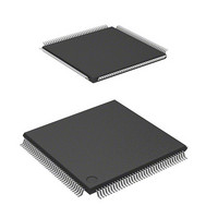
DF2166VTE33 Renesas Electronics America, DF2166VTE33 Datasheet - Page 360

DF2166VTE33
Manufacturer Part Number
DF2166VTE33
Description
MCU FLASH 3V 512K 33MHZ 144TQFP
Manufacturer
Renesas Electronics America
Series
H8® H8S/2100r
Datasheet
1.HS2168EPI61H-U.pdf
(876 pages)
Specifications of DF2166VTE33
Core Processor
H8S/2000
Core Size
16-Bit
Speed
33MHz
Connectivity
I²C, IrDA, LPC, SCI, SmartCard
Peripherals
POR, PWM, WDT
Number Of I /o
106
Program Memory Size
512KB (512K x 8)
Program Memory Type
FLASH
Ram Size
40K x 8
Voltage - Supply (vcc/vdd)
3 V ~ 3.6 V
Data Converters
A/D 8x10b; D/A 2x8b
Oscillator Type
External
Operating Temperature
-20°C ~ 75°C
Package / Case
144-TQFP, 144-VQFP
Lead Free Status / RoHS Status
Contains lead / RoHS non-compliant
Eeprom Size
-
- Current page: 360 of 876
- Download datasheet (5Mb)
• TCSR_X
Rev. 3.00, 03/04, page 318 of 830
Bit
7
6
5
4
3
2
This register can be accessed when the KINWUE bit in SYSCR is 0 and the TMRX/Y bit in
TCONRS is 0.
Bit Name Initial Value R/W
OS3
OS2
CMFB
CMFA
OVF
ICF
0
0
0
0
0
0
R/(W)* Compare-Match Flag B
R/(W)* Compare-Match Flag A
R/(W)* Timer Overflow Flag
R/(W)* Input Capture Flag
R/W
R/W
Description
[Setting condition]
When the values of TCNT_X and TCORB_X match
[Clearing condition]
Read CMFB when CMFB = 1, then write 0 in CMFB
[Setting condition]
When the values of TCNT_X and TCORA_X match
[Clearing condition]
Read CMFA when CMFA = 1, then write 0 in CMFA
[Setting condition]
When TCNT_X overflows from H'FF to H'00
[Clearing condition]
Read OVF when OVF = 1, then write 0 in OVF
[Setting condition]
When a rising edge and falling edge is detected in
the external reset signal in that order.
[Clearing condition]
Read ICF when ICF = 1, then write 0 in ICF
Output Select 3 and 2
These bits specify how the TMOX pin output level is
to be changed by compare-match B of TCORB_X
and TCNT_X.
00: No change
01: 0 is output
10: 1 is output
11: Output is inverted (toggle output)
Related parts for DF2166VTE33
Image
Part Number
Description
Manufacturer
Datasheet
Request
R

Part Number:
Description:
0.6mm Pitch Board-to-Fine-Coaxial Cable Connectors
Manufacturer:
Hirose Electric
Datasheet:

Part Number:
Description:
0.6mm Pitch Board-to-fine-coaxial Cable Connectors
Manufacturer:
Hirose Electric
Datasheet:

Part Number:
Description:
0.6mm Pitch Board-to-fine-coaxial Cable Connectors
Manufacturer:
Hirose Electric
Datasheet:

Part Number:
Description:
Right angle, Two-piece for fine coaxial cable, Discrete wire connectors; HRS No: 687-0001-5 56; No. of Positions: 20; Connector Type: Board mounting; Contact Gender: Female; Contact Spacing (mm): 0.6; Terminal Pitch (mm): 0.6; PCB Mount Type: SMT; Cu
Manufacturer:
Hirose Electric

Part Number:
Description:
0.6mm Pitch Board-to-fine-coaxial Cable Connectors
Manufacturer:
Hirose Electric
Datasheet:

Part Number:
Description:
0.6mm Pitch Board-to-Fine-Coaxial Cable Connectors
Manufacturer:
HIROSE [Hirose Electric]
Datasheet:

Part Number:
Description:
KIT STARTER FOR M16C/29
Manufacturer:
Renesas Electronics America
Datasheet:

Part Number:
Description:
KIT STARTER FOR R8C/2D
Manufacturer:
Renesas Electronics America
Datasheet:

Part Number:
Description:
R0K33062P STARTER KIT
Manufacturer:
Renesas Electronics America
Datasheet:

Part Number:
Description:
KIT STARTER FOR R8C/23 E8A
Manufacturer:
Renesas Electronics America
Datasheet:

Part Number:
Description:
KIT STARTER FOR R8C/25
Manufacturer:
Renesas Electronics America
Datasheet:

Part Number:
Description:
KIT STARTER H8S2456 SHARPE DSPLY
Manufacturer:
Renesas Electronics America
Datasheet:

Part Number:
Description:
KIT STARTER FOR R8C38C
Manufacturer:
Renesas Electronics America
Datasheet:

Part Number:
Description:
KIT STARTER FOR R8C35C
Manufacturer:
Renesas Electronics America
Datasheet:

Part Number:
Description:
KIT STARTER FOR R8CL3AC+LCD APPS
Manufacturer:
Renesas Electronics America
Datasheet:


